 |
|
Projects: Extending Machine Instructions
|
|
|
Instruction examples Sideband effects
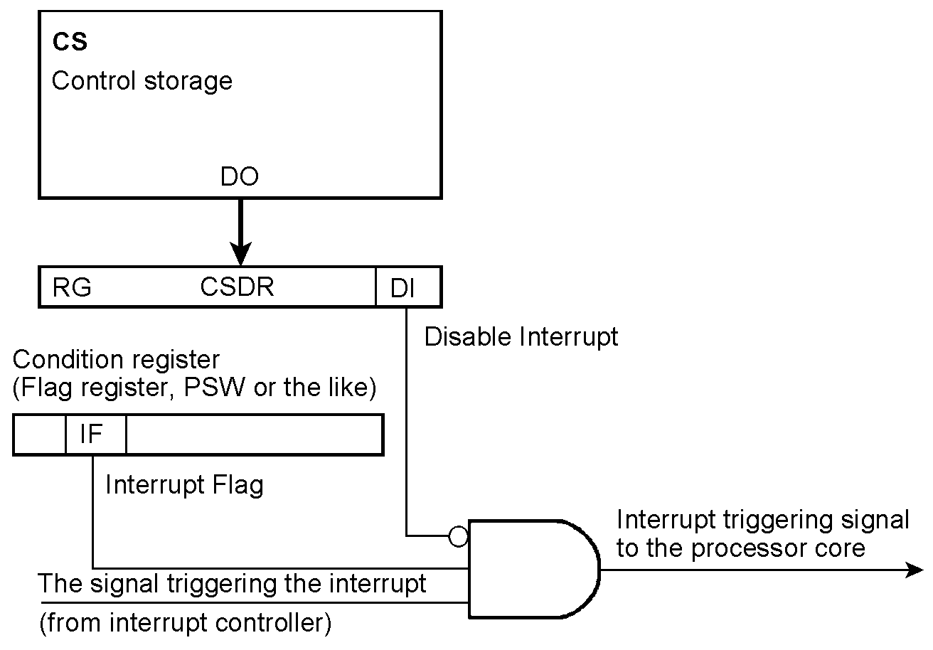
Disabling interrupts temporarily
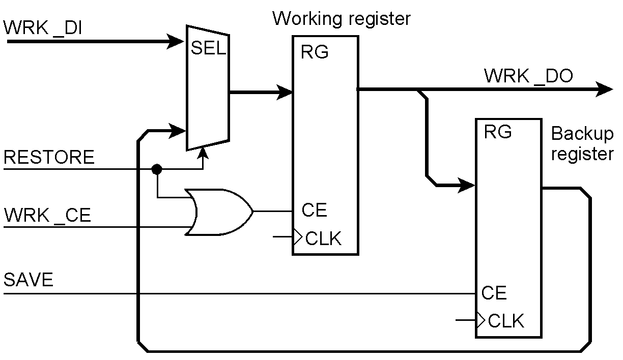
Loading registers
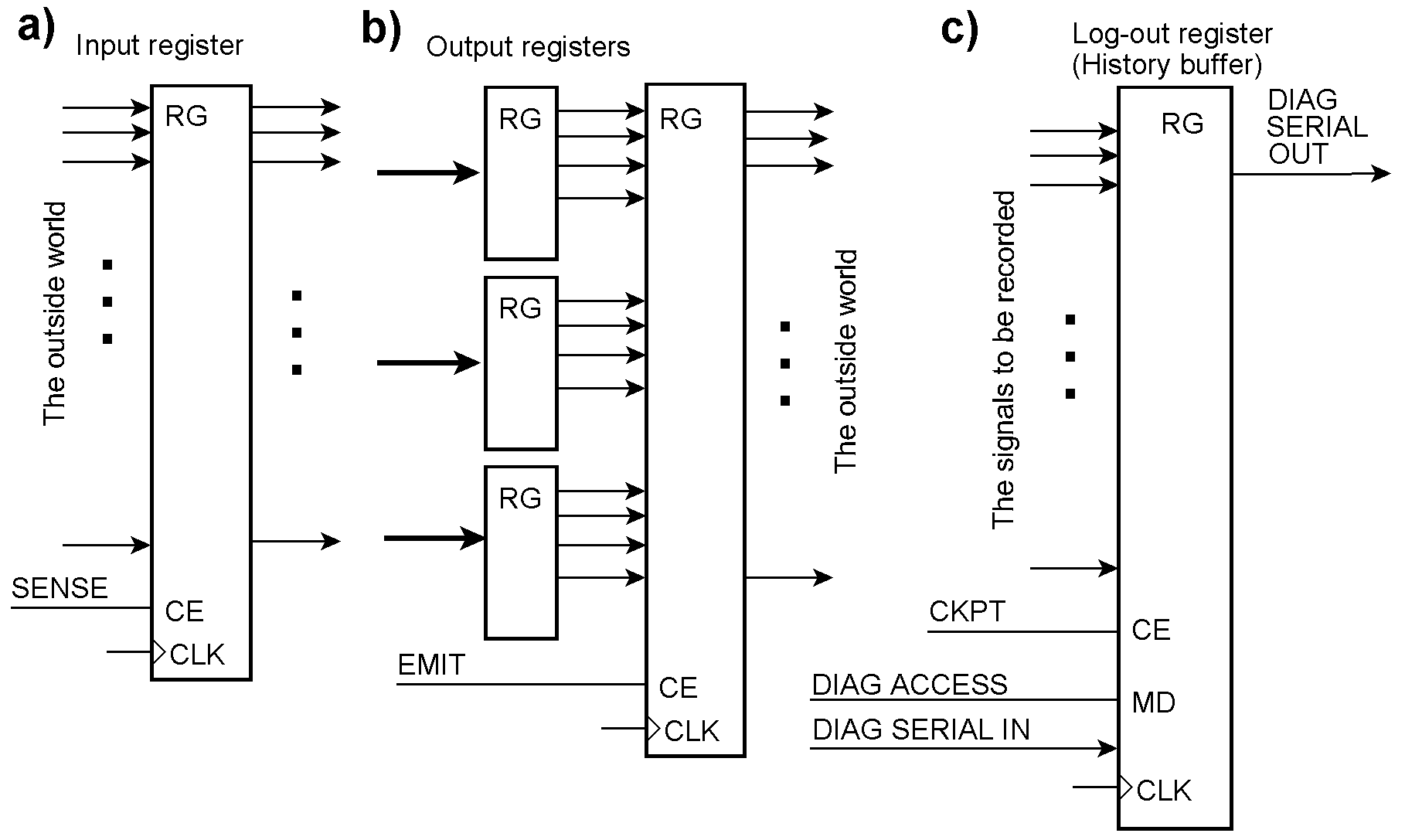
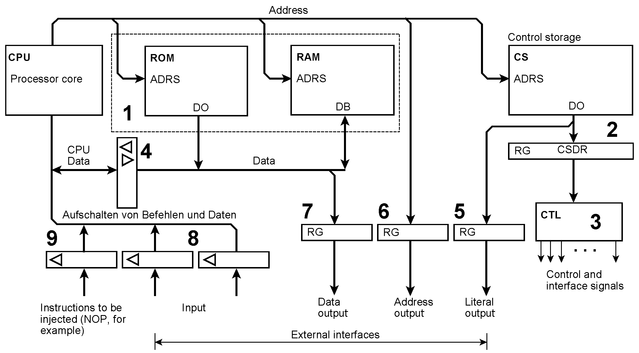
Micro-orders cause various registers to be loaded. SENSE captures data from the outside world (a), and EMIT causes the contents of various output registers to appear in the outside world at once (b). CKPT (Checkpoint) loads signals to be saved for debugging or error handling into a log-out register or history buffer, respectively (c). In this example, it is read out serially.
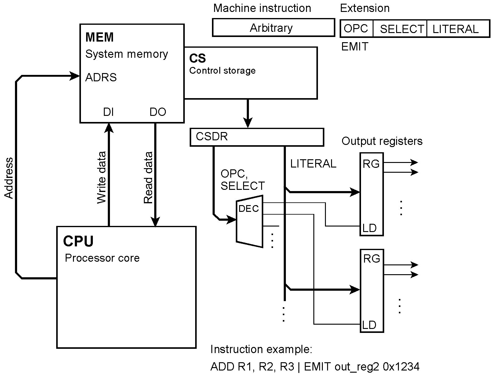
Emit ouput data
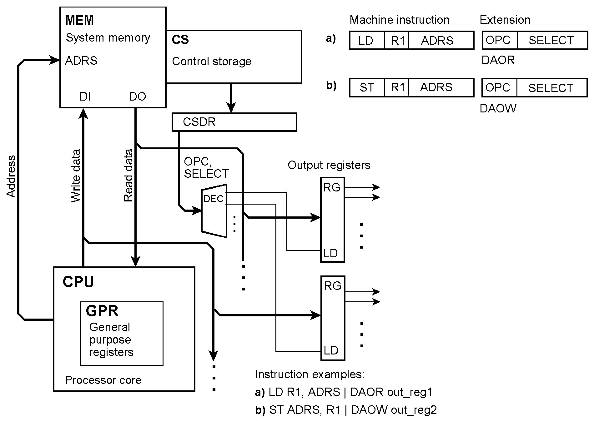
Concurrent output The microinstruction taps the data the processor reads out from or writes into the memory, respectively. OPC = the extension’s opcode; SELECT = output register selection; DAOR = Data Output while Reading; DAOW = Data Output while Writing. In instruction example (a), a load instruction causes the addressed memory content to be loaded into the output register out_reg1 too. In instruction example (b), a store instruction causes the data to be stored to be loaded into the output register out_reg2 too.
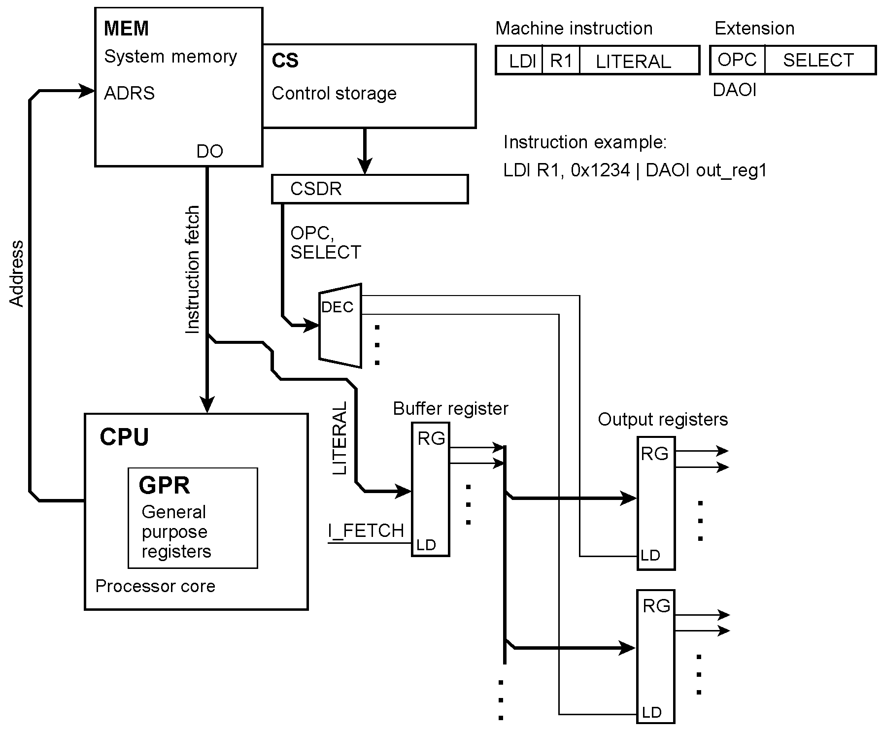
The microinstruction taps the immediate value (literal) contained in the instruction. Because the literal appears during instruction fetch, it must be buffered. OPC = the extension’s opcode; SELECT = output register selection ; DAOI = Data Output Immedate. In the instruction example, a load immediate instruction causes the immediate value (literal) to be loaded into the output register out_reg1 too.
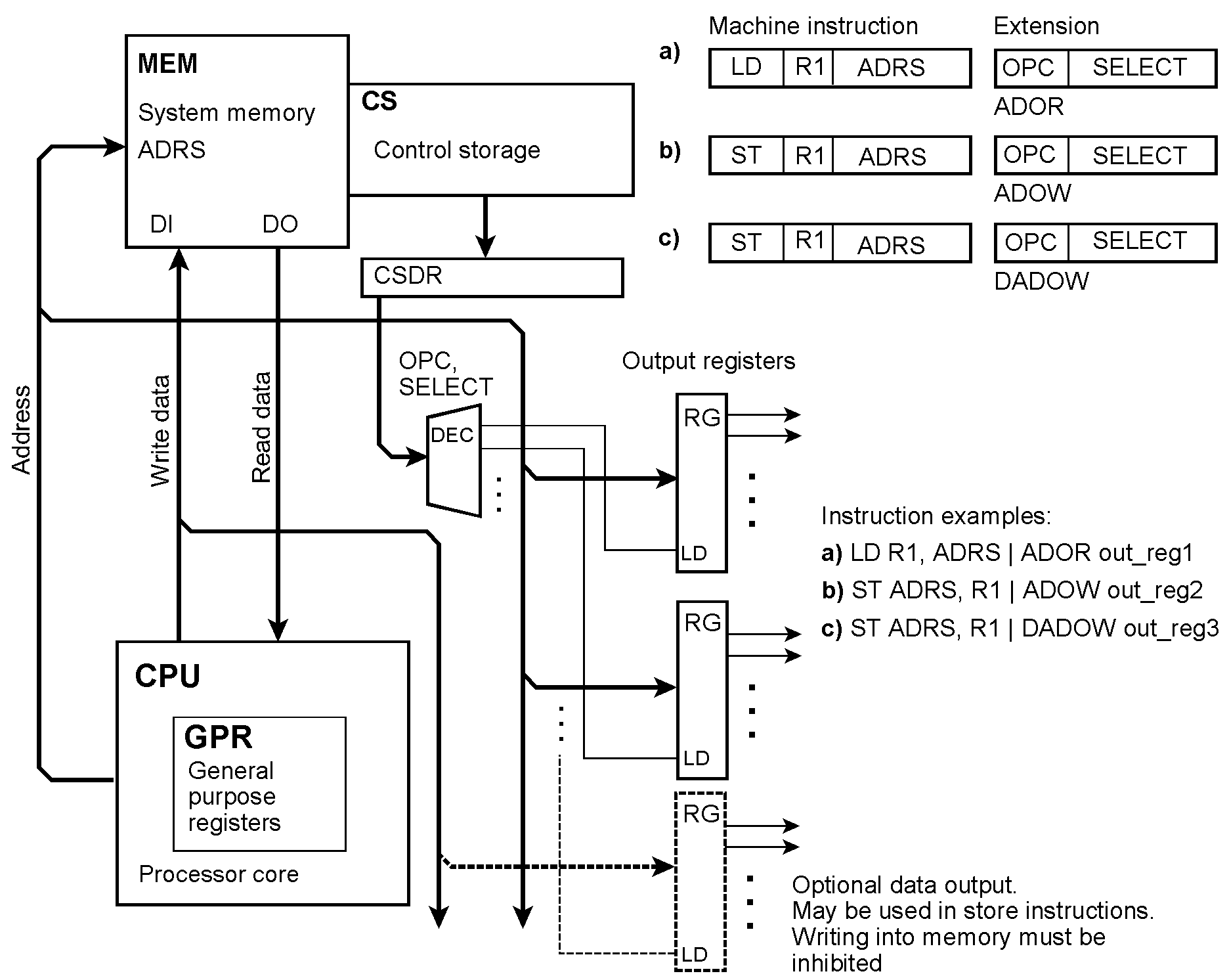
Even the memory address could be output The micronstruction taps the memory address too. OPC = the extension’s opcode; SELECT = output register selection ; ADOR = Address Output while Reading; ADOW = Address Output while Writing; DADOW = Data and Address Output while Writing. In both instruction examples (a) and (b), a load or store instruction causes the memory address loaded into an output register. In the instruction example (c), a store instruction causes the the address and the data to be stored to be loaded into two output registers, addressed by out_reg3.
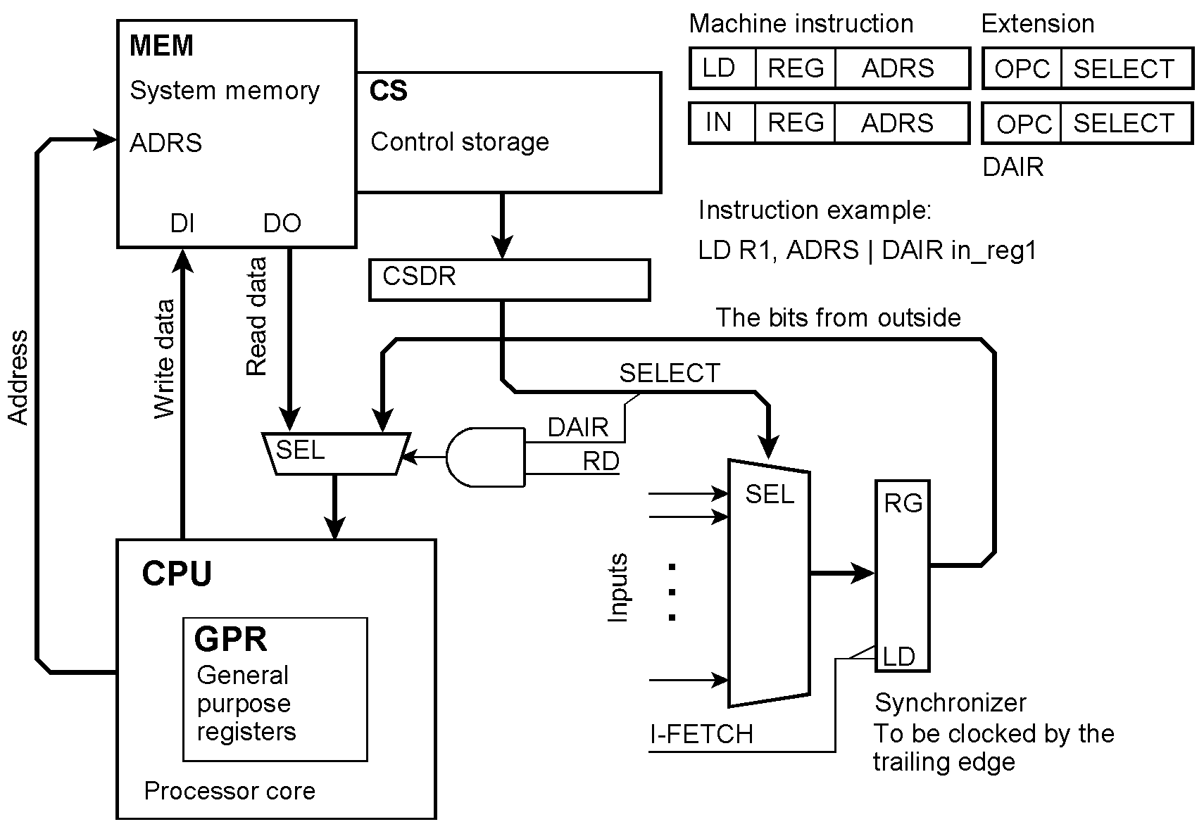
Input by injecting data Input data are to be injected during a read cycle if they are to be delivered to the processor, or during a write cycle if they are to be written into the memory. Data coming from outside must be synchronized before being fed into a data path. Input data are read into the processor core. OPC = the extension’s opcode; SELECT = output register selection; DAIR = Data Input while Reading. In the instruction example, during the data access of a load instruction, the content of the input register in_reg1 will be injected into the data path and thus loaded into the destination register R1 instead of the addressed memory content.
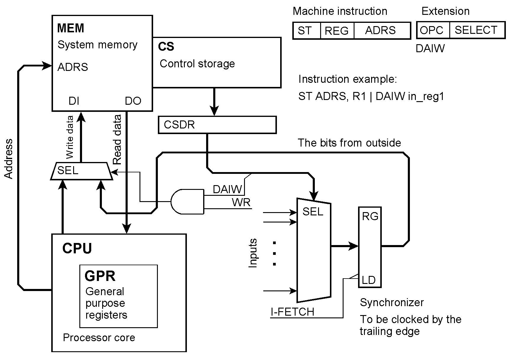
Input data are written into the memory. OPC = the extension’s opcode; SELECT = output register selection; DAIW = Data Input while Writing. In the instruction example, during the data access of a write instruction, the content of the input register in_reg1 will be injected into the data path and thus written into the memory instead of the processor’s register content.
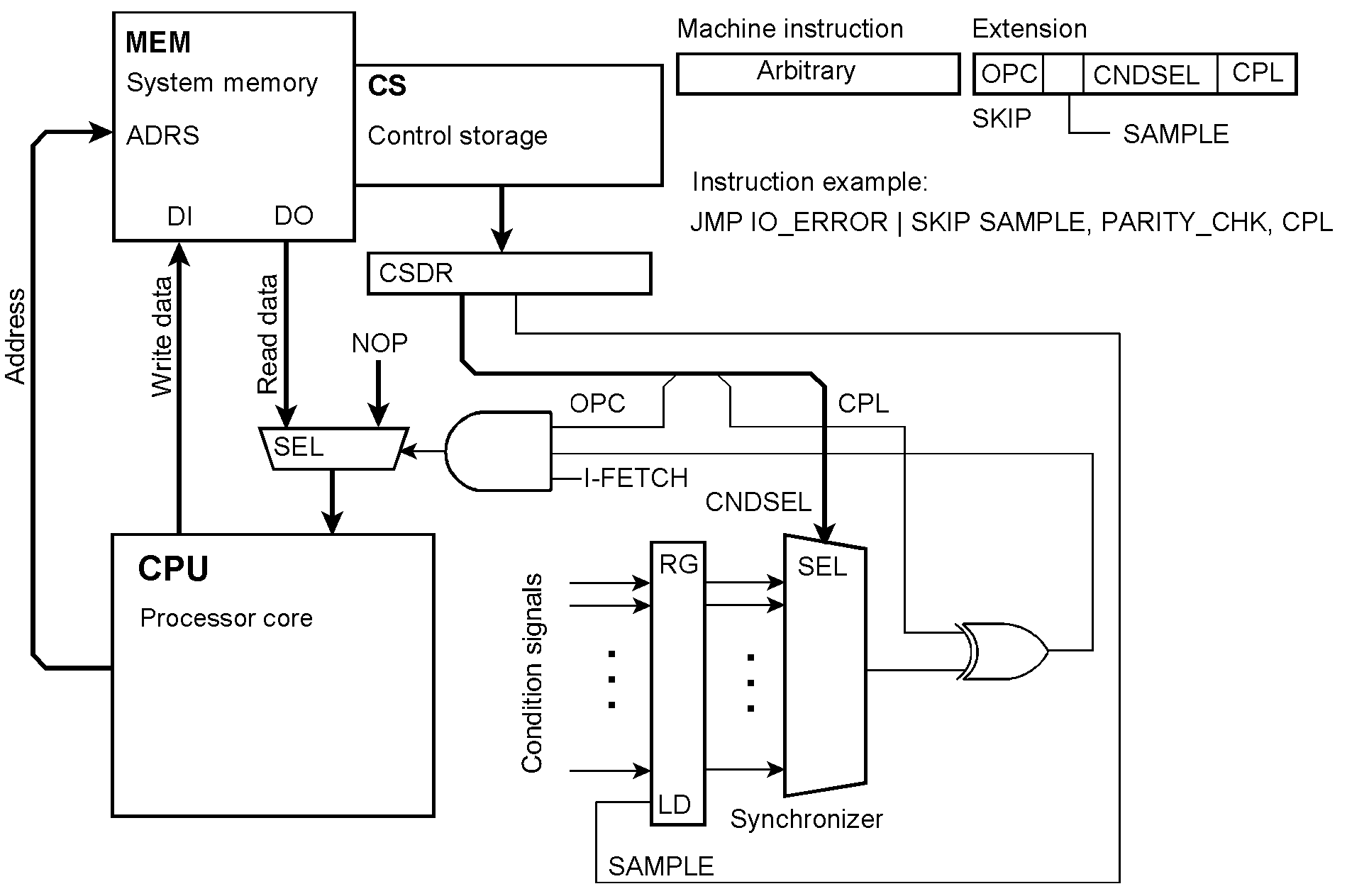
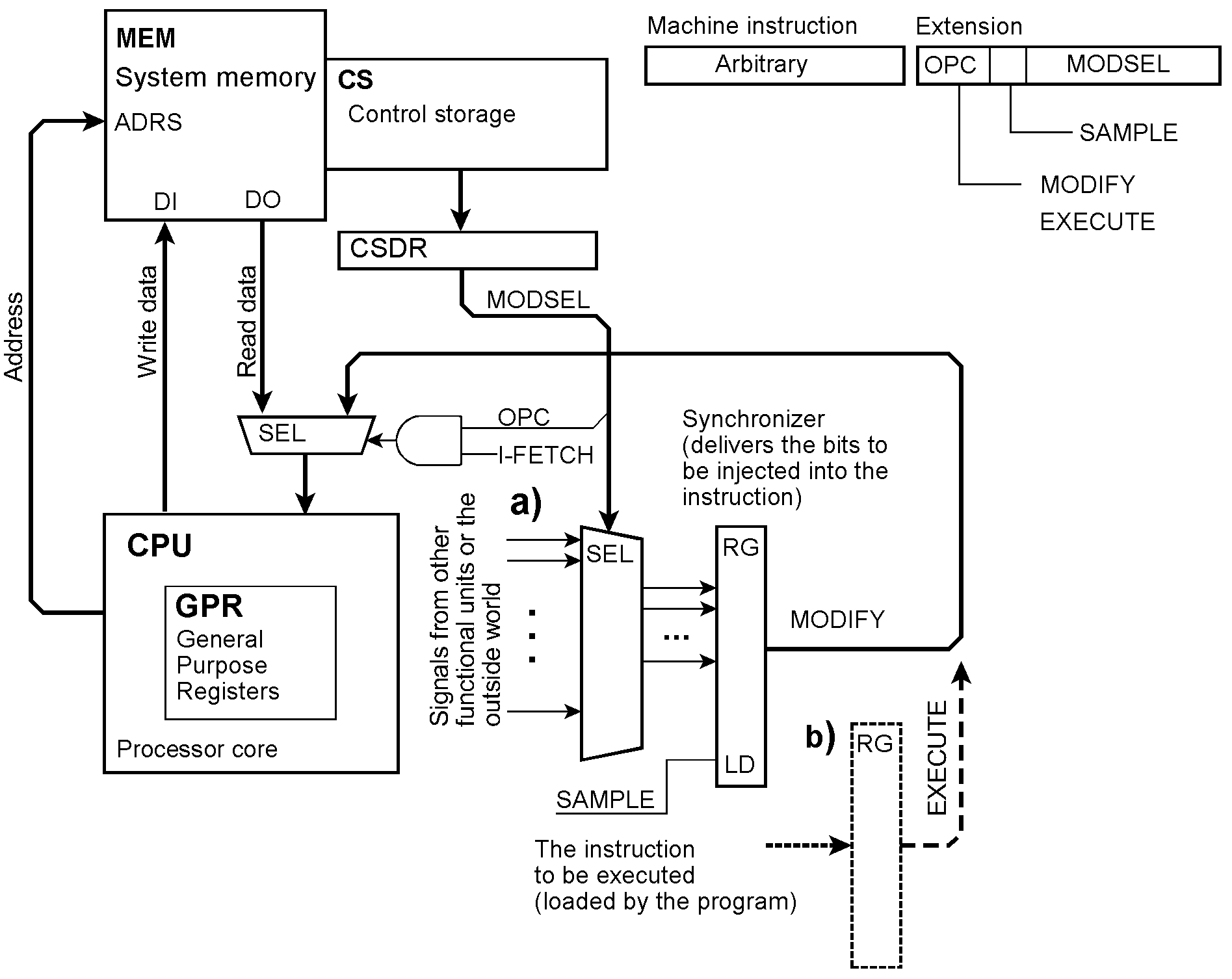
Executing instructions conditionally Our predicates are conditions selected from the outside world. In contrast to some well-known architectures, we are not limited to the content of a predicate register or a few condition bits but can select any number of predicates from arbitrary sources. A branch on condition is programmed by an unconditional jump accompanied by the appropriate extension. The details of the implementation are somewhat tricky. The extension may belong to the instruction that is to be executed conditionally (as shown in Figure 13). Because the condition can be selected no more early than at the beginning of the instruction fetch cycle, it could be necessary to insert a wait state. Alternatively, the extension could accompany the previous instruction. Then we have to ensure that interrupts between these two instructions are inhibited. If the condition is not satisfied, the processor core will receive a NOP instead of the instruction and thus skip it. OPC = the extension’s opcode; SAMPLE = capture the conditions; CNDSEL = condition selection; CPL = complement (invert) the condition. In the instruction example, a jump to an error-handling routine will be skipped if no parity check has been detected. If more than one instruction is to be executed conditionally, the condition must be captured at the beginning of this instruction block and then kept. To this end, latching (sampling) the conditions is controlled by the SAMPLE microinstruction bit.
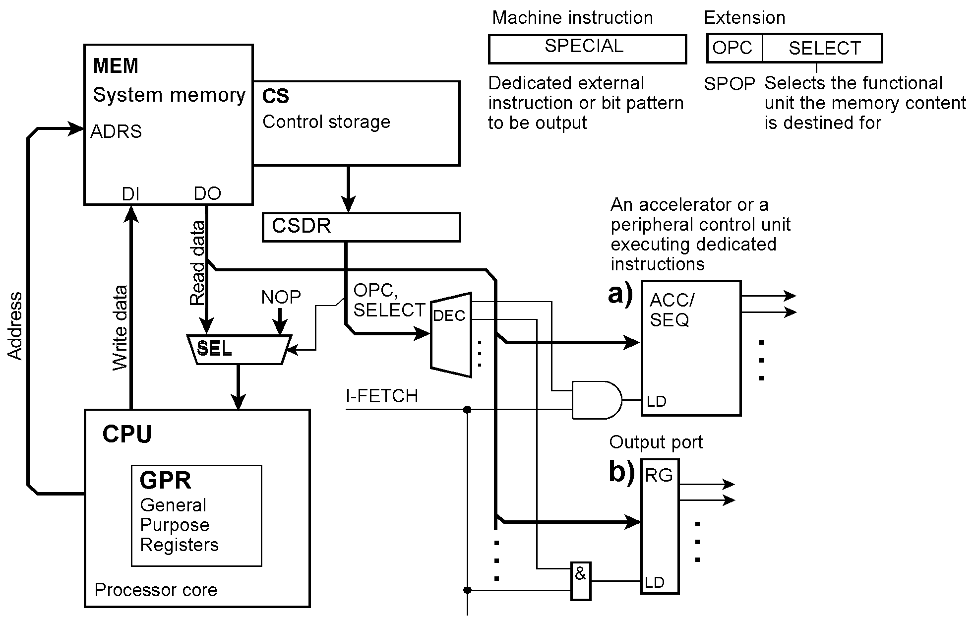
Injecting NOPs and other instructions Outputting instructions instead of executing them Instructions extended this way never make it into the processor. It will receive NOPs instead. So the memory may contain arbitrary bit patterns. They may serve as special instructions (a) of an accelerator or a peripheral control unit or may be output immediately (b).
Injecting modified or completely other instructions The EXEC instruction Modifying or substituting instructions from outside. Bits or bit fields of the instruction may be injected (a). Think, for example, of an address field or a literal value set or modified according to external conditions. Complete instructions could also be injected (b). Here a program-accessible register is shown to be loaded with an instruction that has been assembled by the application program. Injecting such an instruction is equivalent to the EXECUTE instruction provided in some legacy architectures. We could also think of supplying a complete instruction from outside, for example, from another processor in a multiprocessor system.
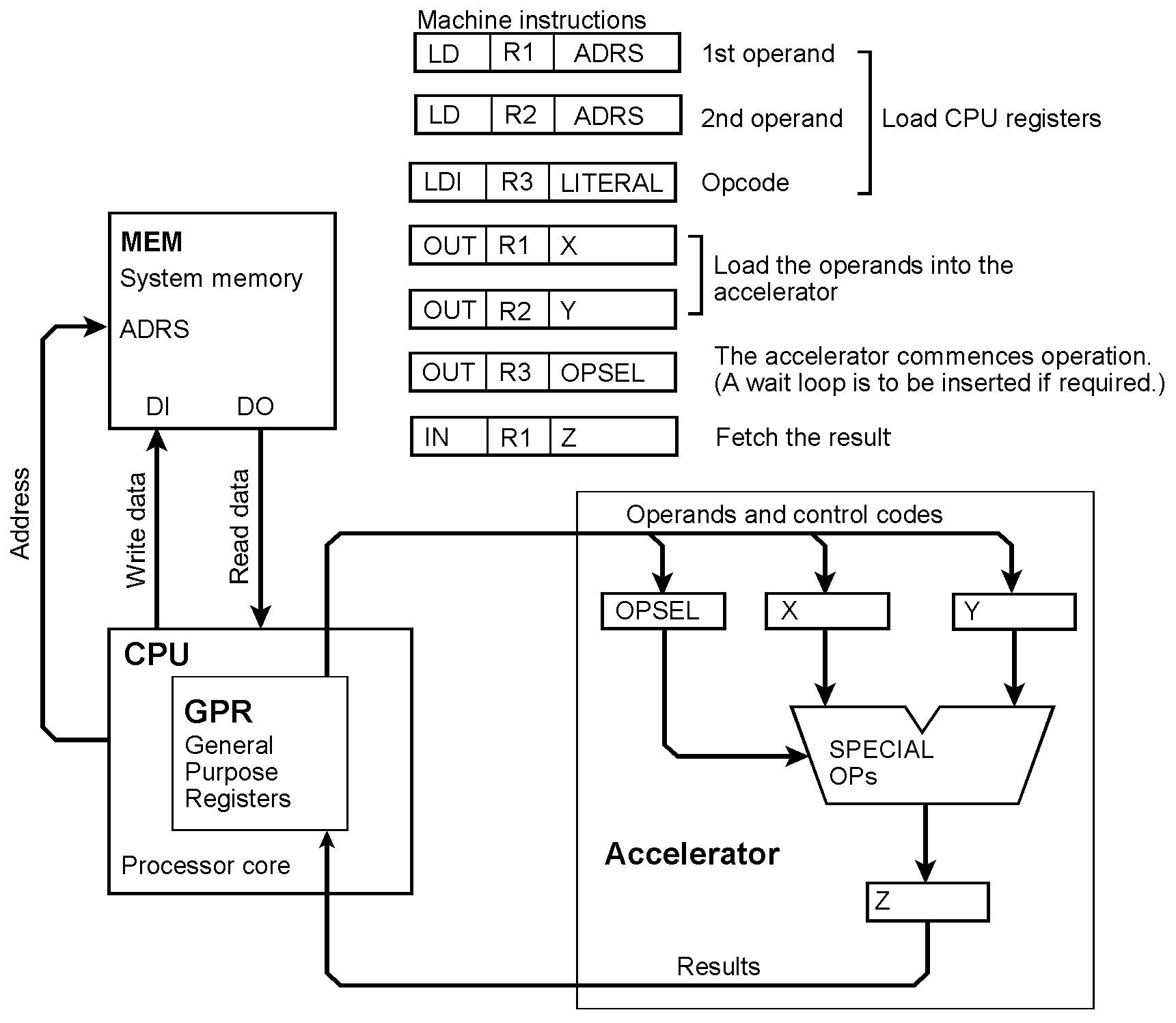
Attaching an accelerator The accelerator is an autonomous device with program-accessible registers at the inputs and outputs. First, the program running in the processor loads the operands into the input registers and starts the operation to be executed. The processor waits for the accelerator to finish. Then it fetches the results. One parameter of an I/O instruction (IN, OUT) addresses a processor register, the other is an I/O address selecting a register in the accelerator.
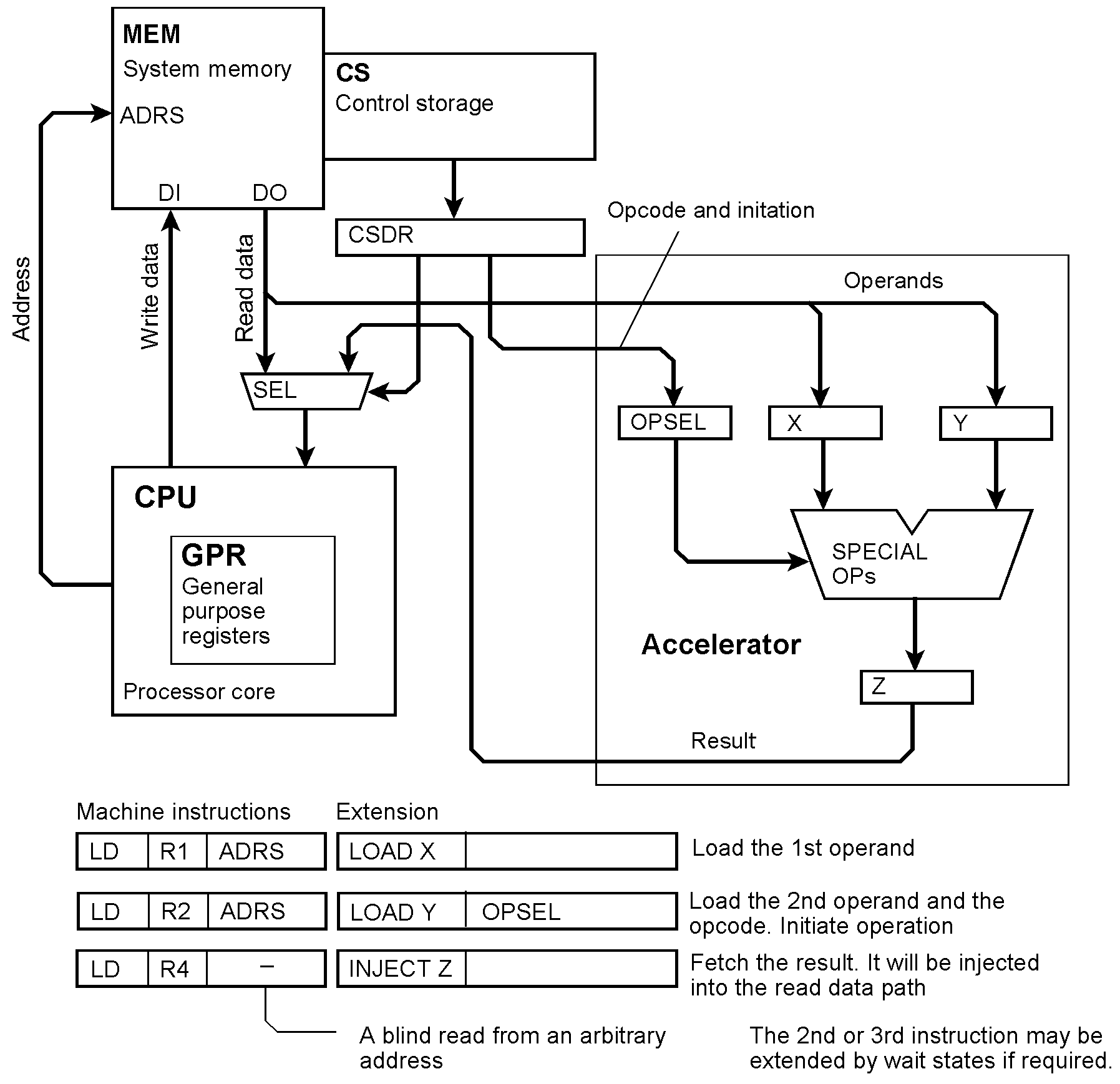
In our alternative solution, machine instructions are extended outside the processor so that they act like microinstructions. The accelerator is operated by extensions. They accompany instructions that provide the operands, select and initiate the operation and fetch the result. The processor reads the operands from memory and loads them into its registers. At the same time, they are tapped to be loaded into the accelerator’s registers. In our example, the operation will start immediately after the last parameter has been entered. Until the result is available, the processor will be held in a wait state. The last of the extended instructions will fetch the result and load it into a processor register. Thus the software overhead typical of such additional circuitry is eliminated. The accelerator behaves as if it were an inherent part of the processor core instead of some kind of an afterthought.
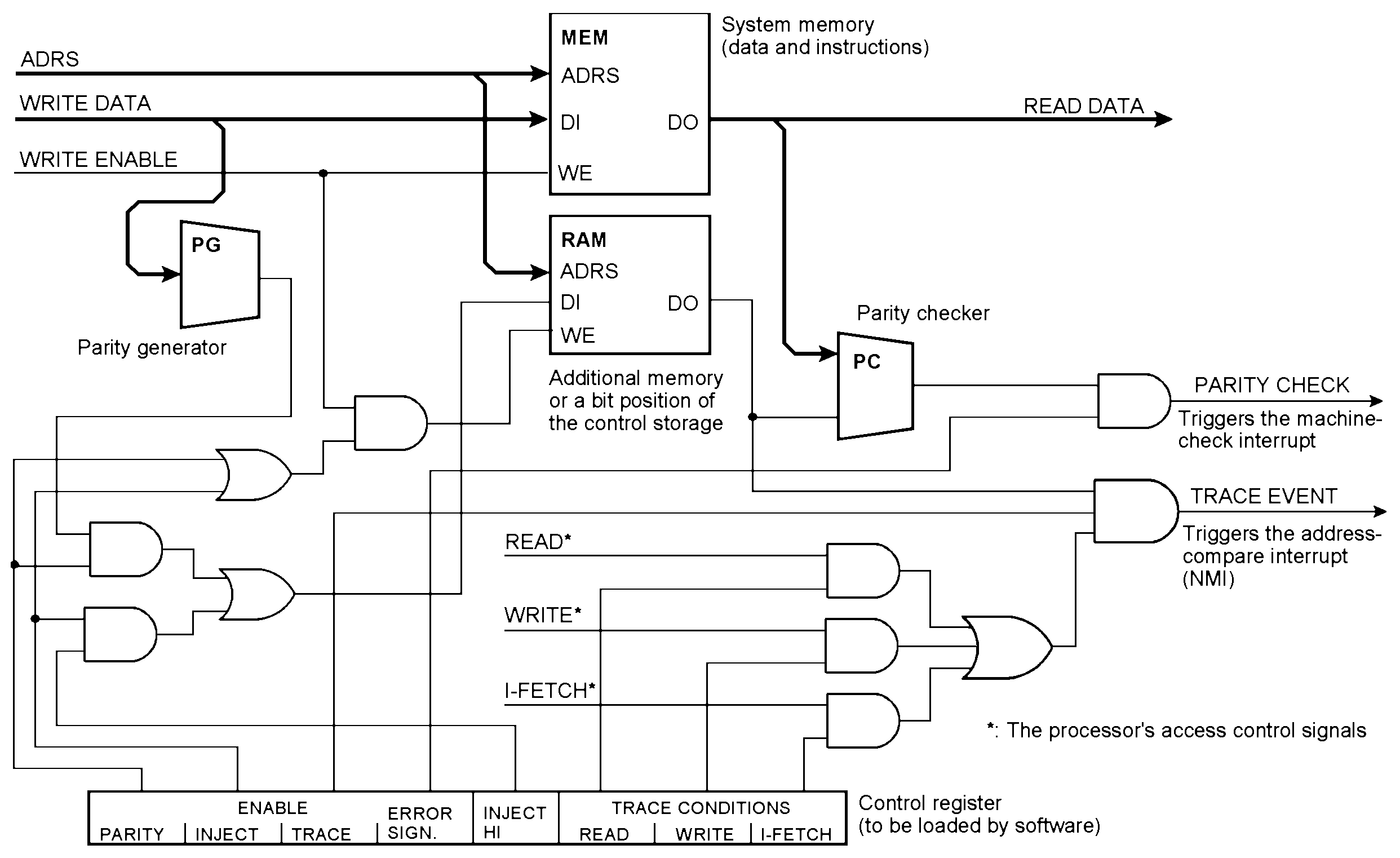
Supporting an unlimited number of breakpoints A bit position in the additional memory causes an address-compare event that triggers an interrupt. If the entire memory is extended this way, you can set any number of breakpoints, up to single-stepping through the instructions. In contrast, the typical built-in breakpoint provisions of microcontrollers support only a few breakpoints (for example, four).
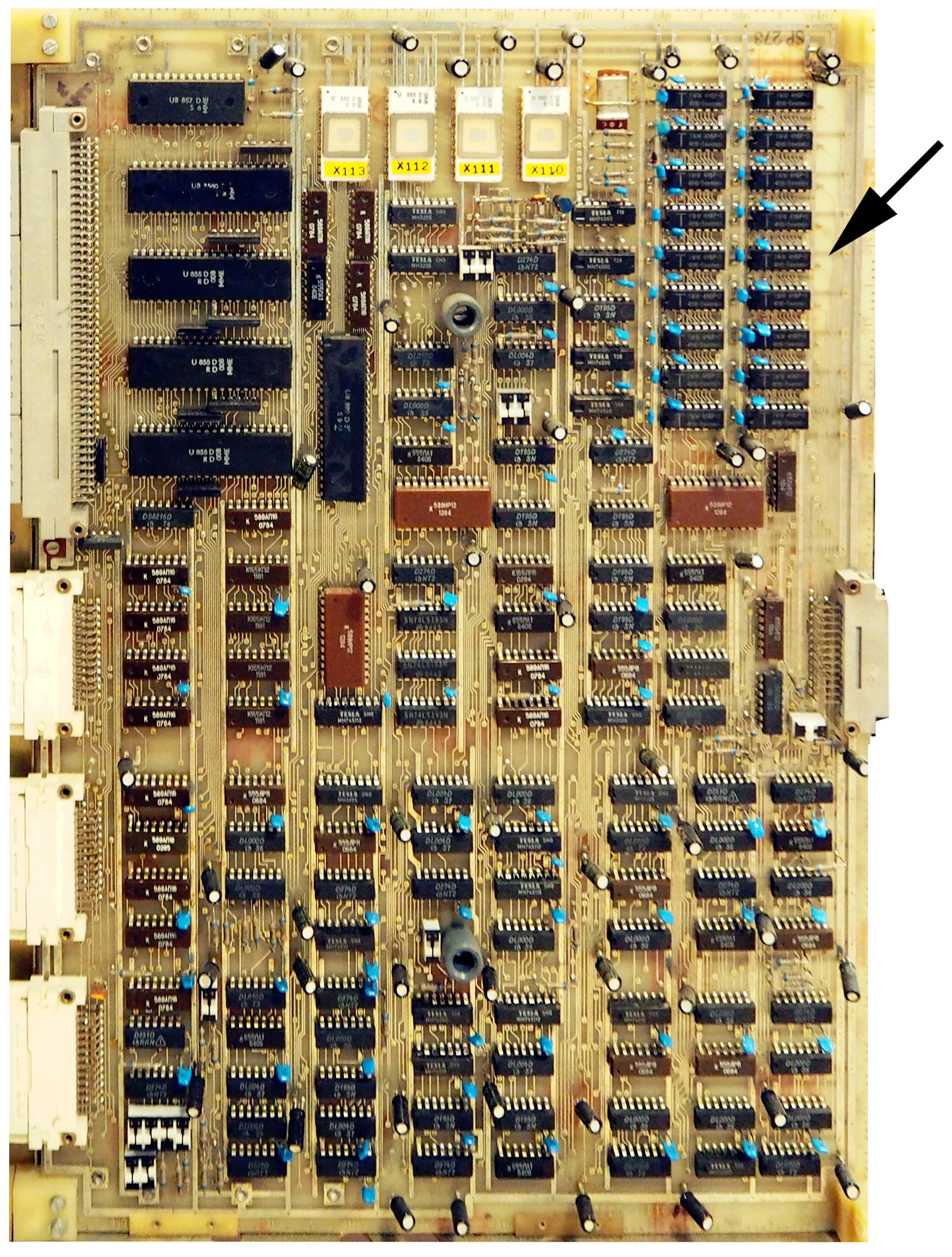
To establish debugging mode, clear the control register and read and rewrite the whole memory content. To set a breakpoint, set INJECT and INJECT HI and read from and write to the desired address. Clear the INJECT bits, set ENABLE TRACE and the desired trace conditions. This is a single-board computer (SBC) out of the Eighties. It features an 9th memory bit, serving as parity or address compare stop bit. Details in [4] and [5]. The arrow points to the 32k • 9 bits DRAM memory, populated by 18 DRAMs of 16 kbits.
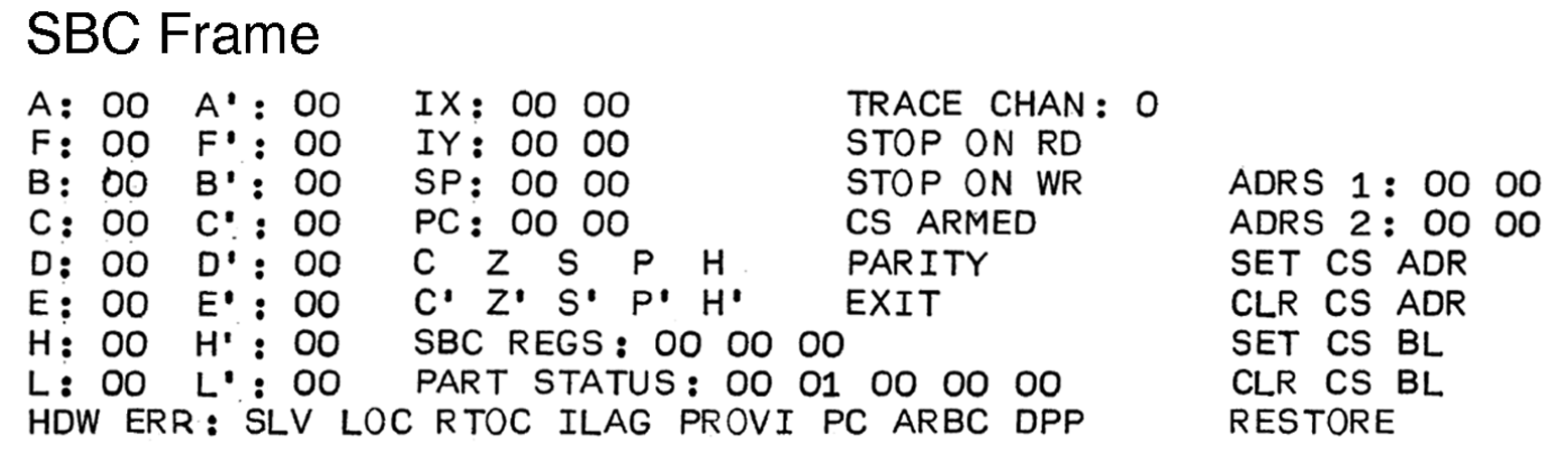
The so-called SBC frame, displayed on a CRT. It allows for viewing and altering the content of the processor’s registers, setting up compare stop modes, and single-stepping through the program. Menu items are selected via cursor keys (no mouse in those bygone times). A selected menu item is displayed inversely (dark characters in a white rectangle). In fields filled with zeros, hexadecimal numbers may be entered.
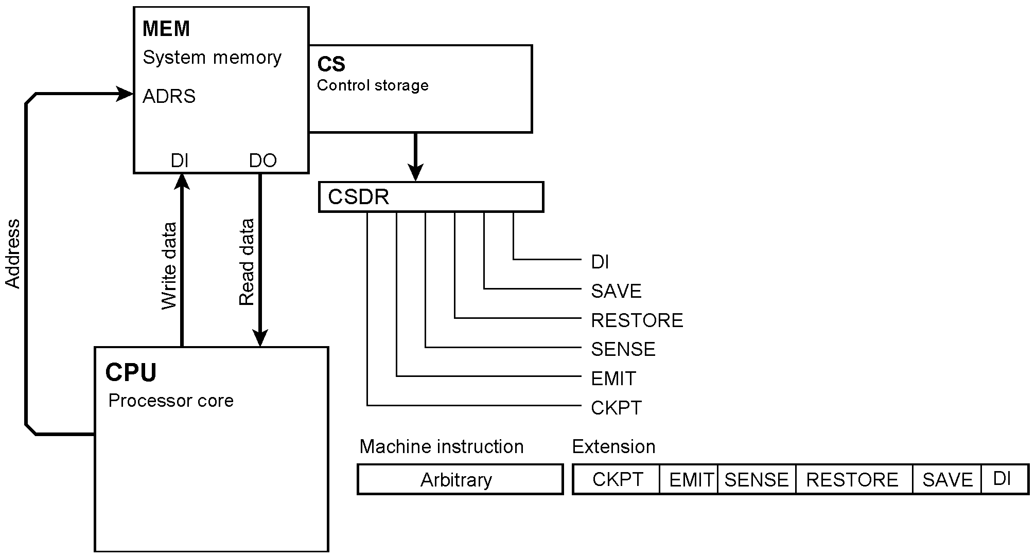
Suitable processor cores Our design ideas have been proven with conventional 8-bit microprocessors. The Zilog Z80, Rockwell 6502, Motrola 6800, and Intel 8051 are historical examples. For Z80-based solutions see [4] to [8]. It should pose no particular difficulty to adapt soft cores like MicroBlaze or NIOS appropriately. With an ARM, MIPS, RISC V, and similar architectures we should be able to implement our proposals provided we choose a suitable processor core. Maybe even high-performance cores could be adapted by appropriately loading page attribute tables, memory type range registers, and the like. In this respect, programs using our extensions can be likened to device drivers controlling the physical I/O circuitry. Accessing the memory Extending a conventional microprocessor system
Back References Project history
|
|
|
|
Download the Internet Addendum to the CC article Download a short synopsis concerning the theory of operation
Download chapter 7. Yes, it is in German. However, an Internet translator should do it. Download three short papers written in the Eighties (under frugal conditions with modest equipment). The examples refer to the Z80 microprocessor. Memory Combines Parity Checking with Program Tracing Support Additional Control Memory Improves Performance of Low-Cost Microprocessors Hardware Support for Testability, Debuging, and Better Performance
Download a synopsis of (more or less) tricky circuitry to be attached to microprocessors, written (of course in German) in the Seventies and Eighties Download an excerpt from this book (in German, despite the title):
|