|
|
|
Designing Pulse Circuits to Solve Application Problems
|
|
|
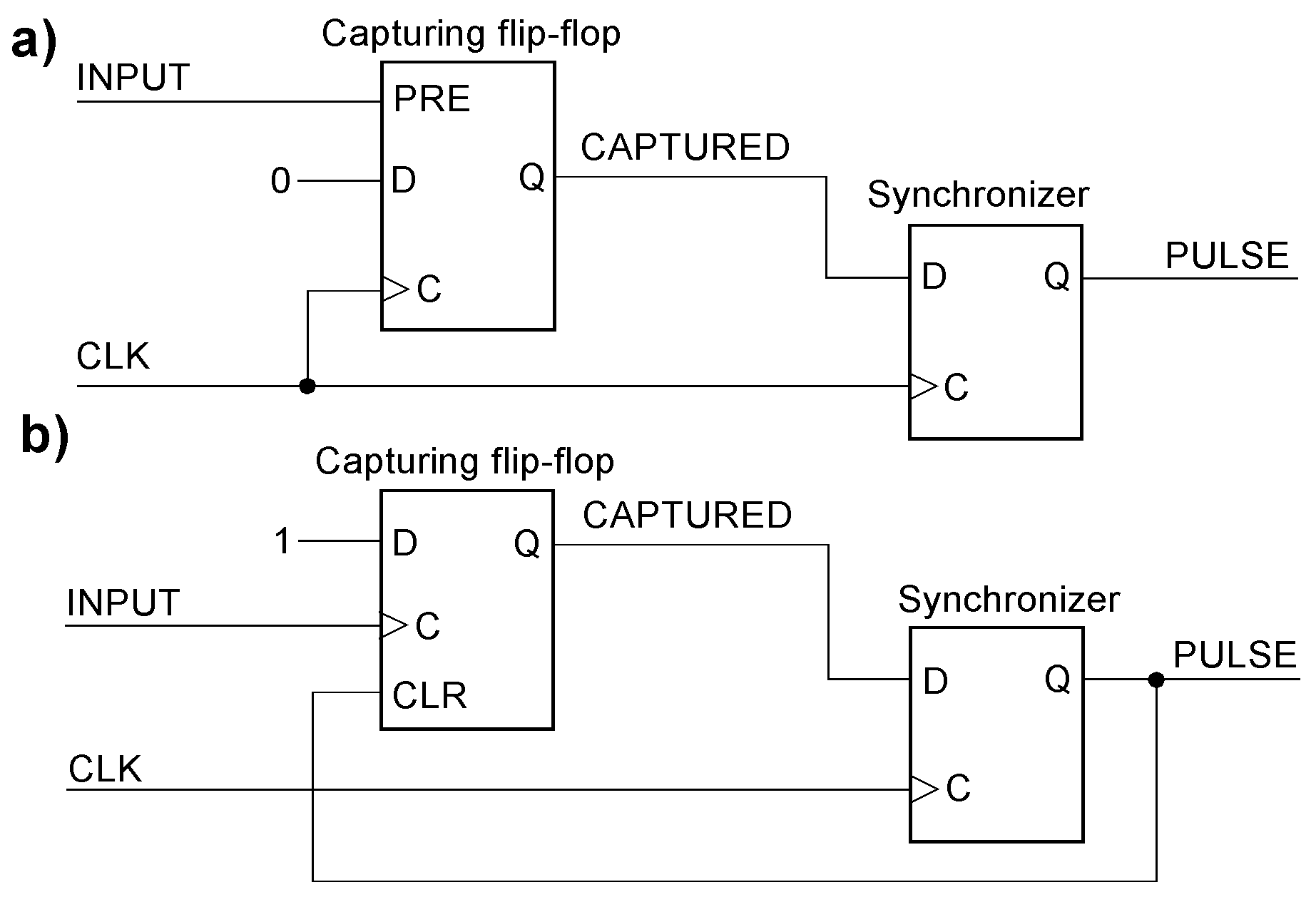
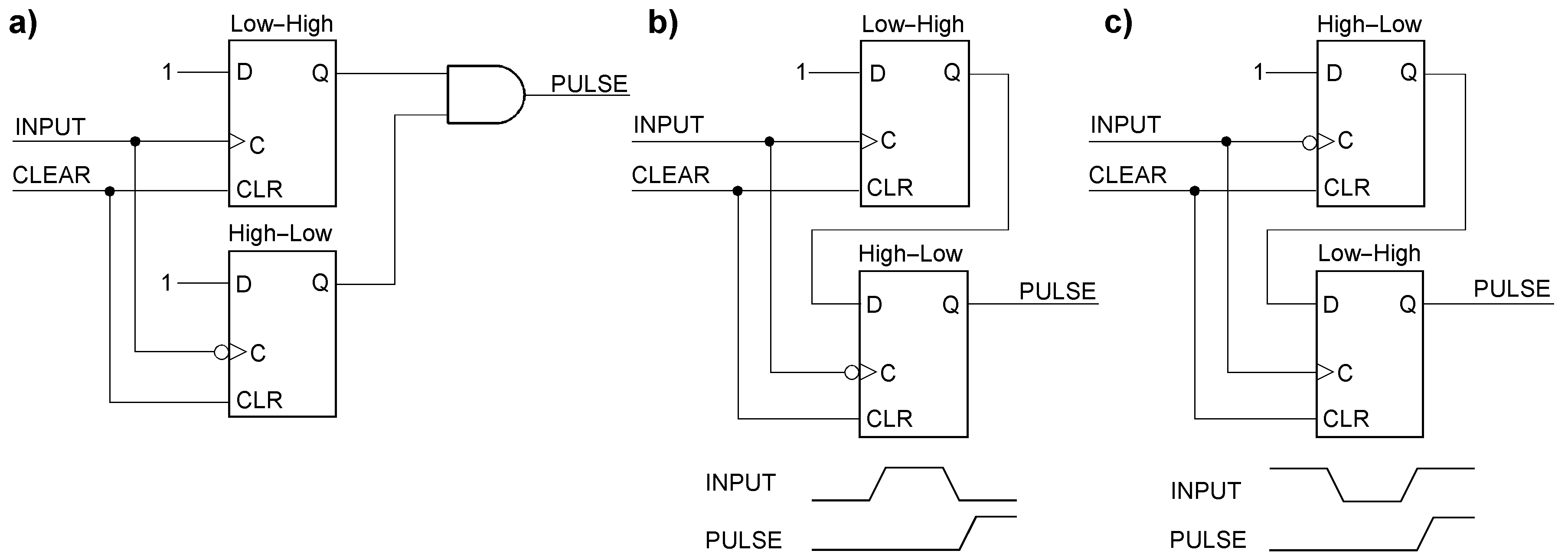
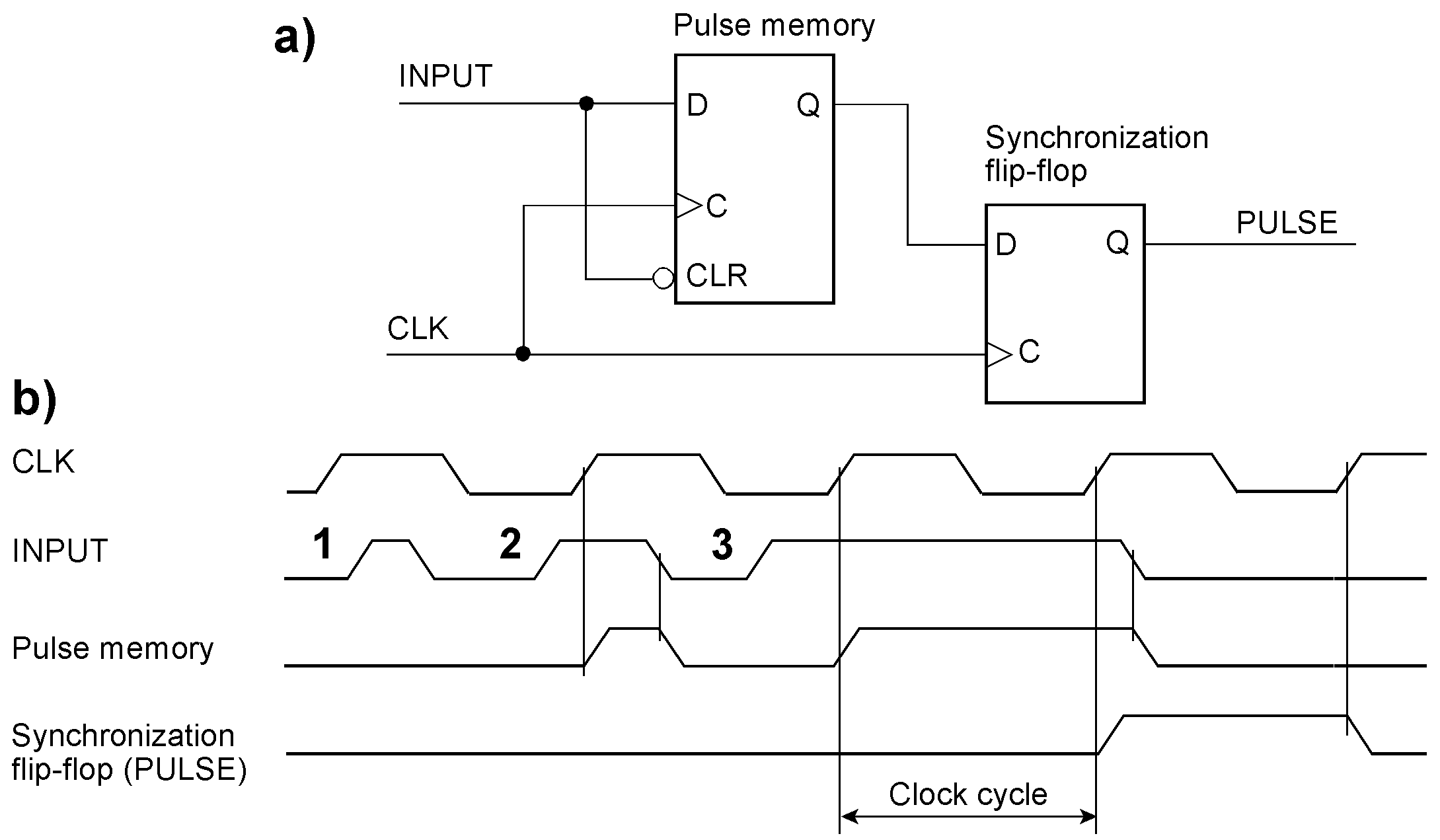
The power-on reset - an introductory note Synchronizing narrow pulses Synchronizing narrow pulses (1). The circuits differ in their behavior when the asynchronous input pulse is wider than a clock cycle (a) or when a new pulse occurs while the synchronizer’s output is still active (b). If the pulses are wider than suggested in the diagram above or follow more closely one another, the circuits will behave differently:
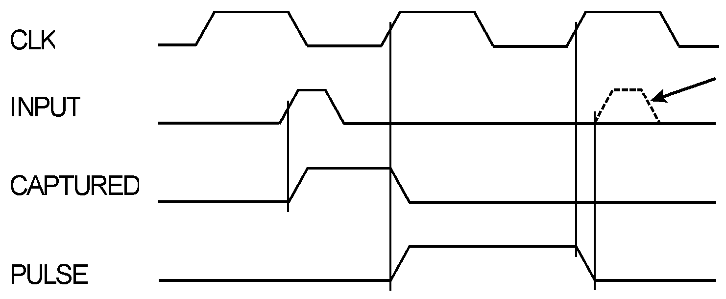
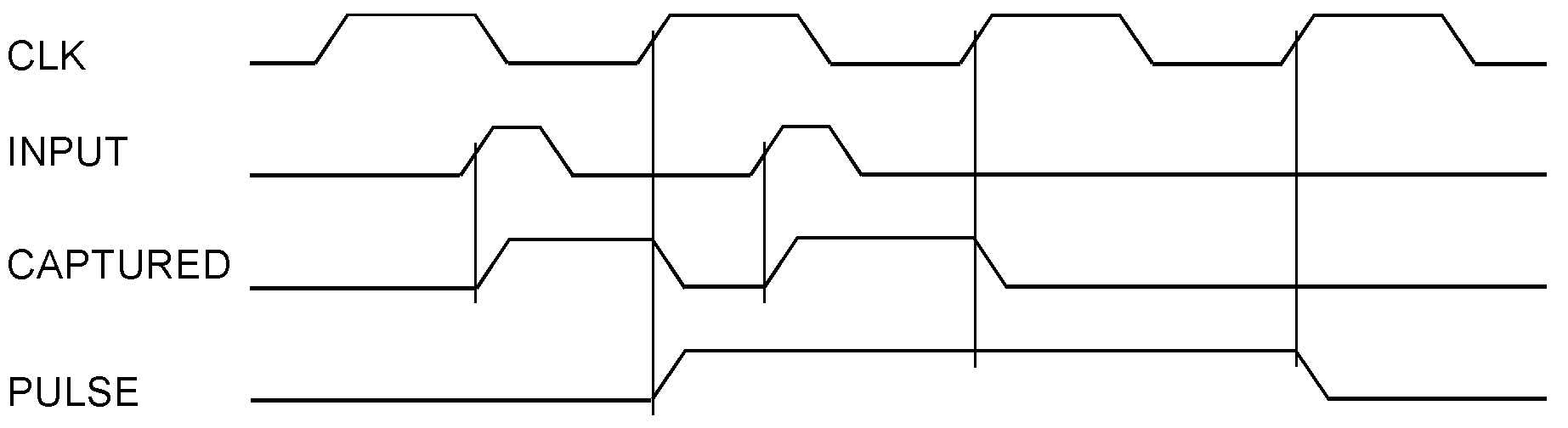
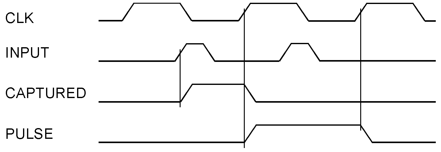
Synchronizing narrow pulses (1). The pulses occur widely apart from one another. The next pulse must not appear before the synchronizer flip-flop has become inactive again (as the arrow points to). Then, the circuits of Figure 1a and 1b behave the same way. Synchronizing narrow pulses (2). The next pulse occurs while the synchronization flip-flop is still active. The level of the input signal takes precedence. Thus, the circuit of Figure 1a will extend the output pulse by another clock cycle. Synchronizing narrow pulses (3). The next pulse occurs while the synchronization flip-flop is still active. The clear signal takes precedence. Thus, the circuit of Figure 1b will ignore the second input pulse.
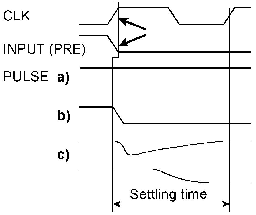
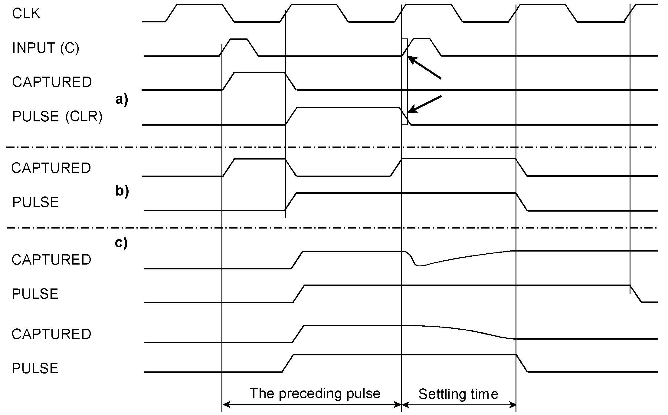
Metastability analysis Metastability problems (1). The coincidence of edges that the arrows point to may occur when the asynchronous input is connected to the PRE (preset) input of the capturing flip-flop. A metastability problem could only occur if the clock goes active while the input becomes inactive . Then, the input may win (that is, the flip-flop sees PRE still as active during the clock edge and hence does not memorize the Low at the D input). Thus, the output remains asserted (a). Alternatively, the clock may win and the output becomes deasserted (b), or there is no winner and the flip-flop goes through a metastable state (c). Metastability problems (2). The coincidence of edges that the arrows point to may occur when the asynchronous input is connected to the CLK (clockt) input of the capturing flip-flop. The clear signal takes precedence over the asynchronous input acting as the flip-flop’s clock. A metastability problem could only occur if the input goes active while the synchronizer’s output becomes inactive. A new pulse occurs in the moment the synchronizer has cleared the preceding pulse memorized by the capturing flip-flop. Therefore, to understand the problem, we must illustrate the history beginning with the previous pulse. If CLR wins, the capturing flip-flop remains deasserted (a). If C wins (that is, the asynchronous pulse input), the capturing flip-flop will switch on again (b), causing the output to remain asserted during the next clock cycle. If there is no winner, the capturing flip-flop goes through a metastable state (c).
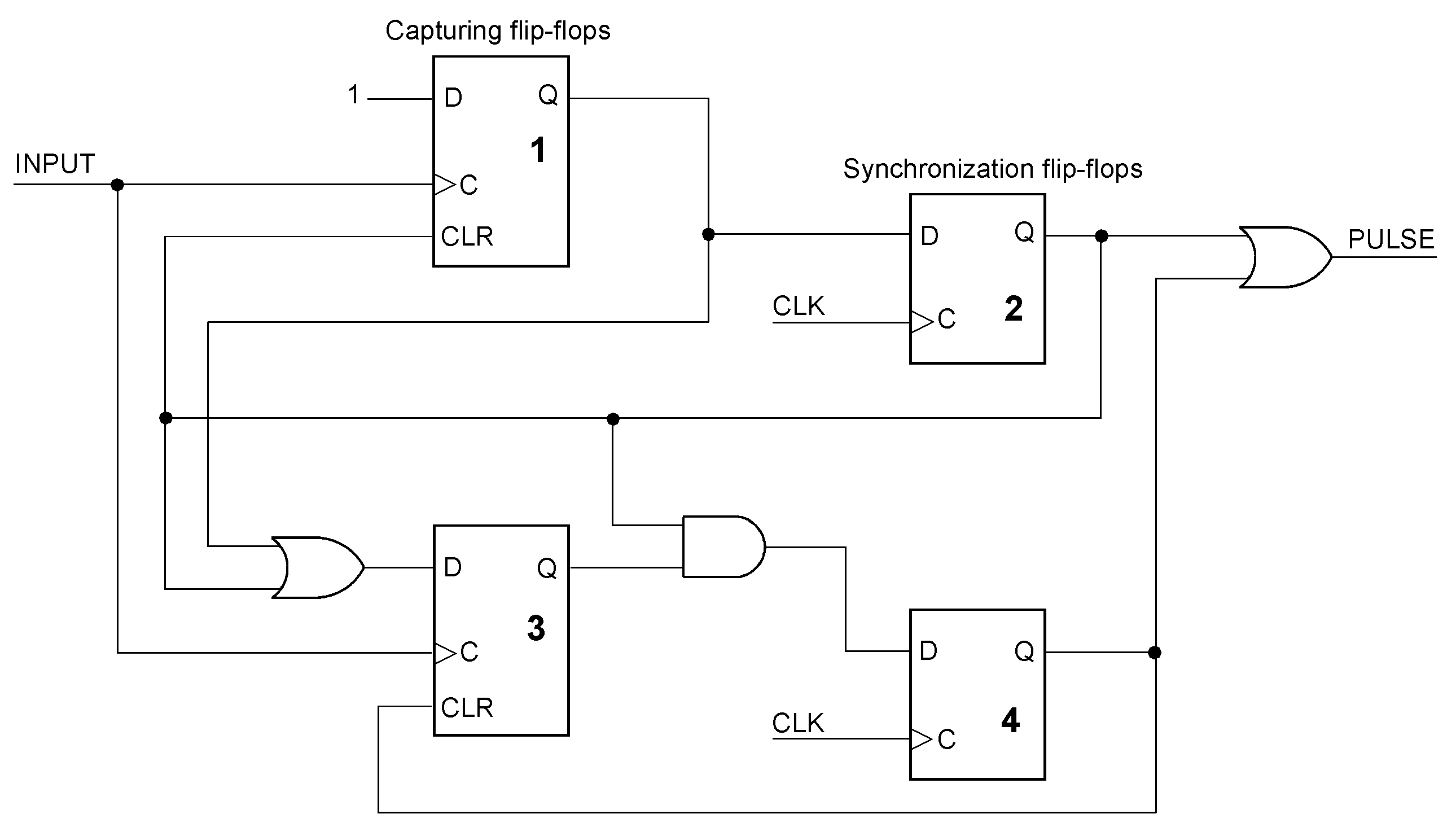
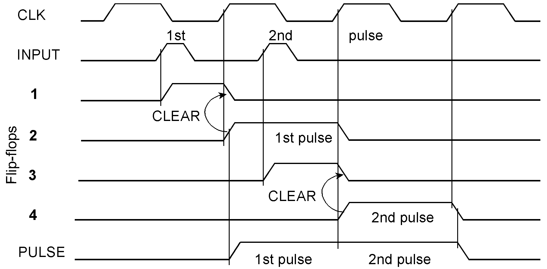
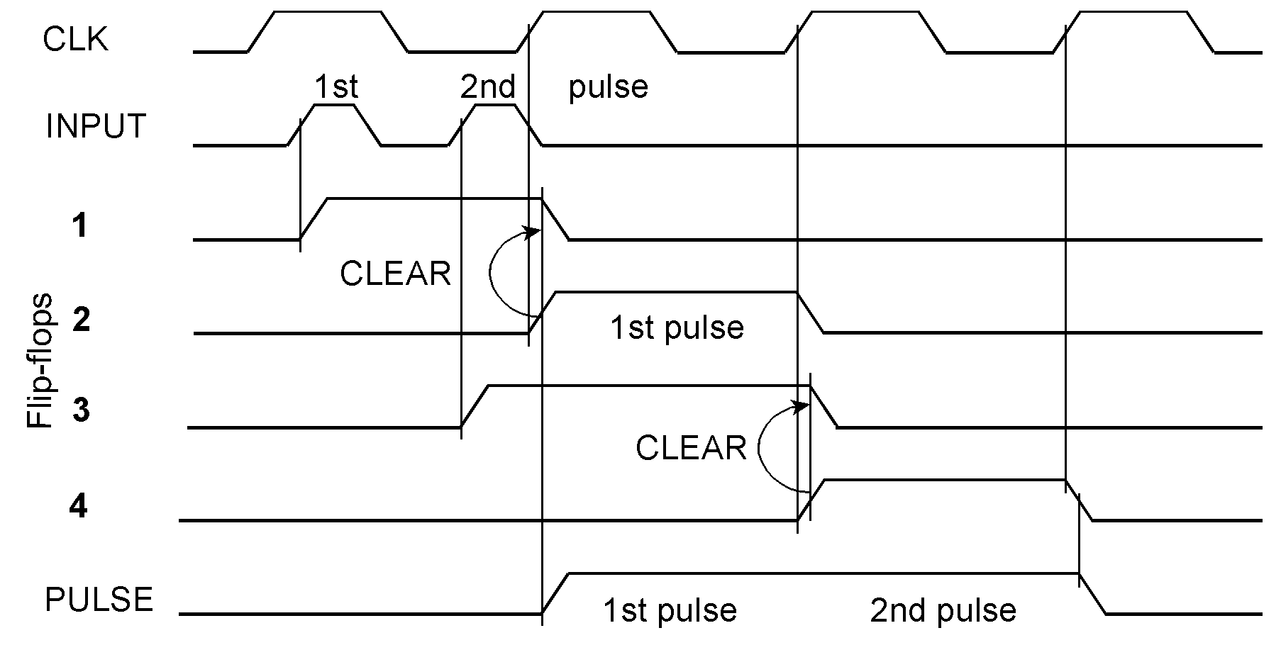
In both circuits, one of the signals whose overlapping could cause metastable states is asserted or deasserted by the synchronizer and hence by a clock edge. Therefore, the settling time always equals one complete clock cycle. So we can assume that the synchronizer will see a settled input level when the next clock cycle begins. As a consequence of the metastable state, it could be Low or High, respectively. Accordingly, the output pulse will end or remain active during the next clock cycle.. Both circuits will perform well if the width of the input pulses surpasses the flip-flop’s pulse width data sheet parameter and the gaps between the pulses are wider than a clock period. Moreover, the clock cycle provides the settling time to prevent failures caused by metastable states. So it should be chosen at least as wide as necessary to ensure the specified MTBF. When not specified, choose a reasonable magnitude, perhaps some centuries. The problem has been discussed in the preceding article [3]. Synchronize pulses continuously Continuous synchronization with two capturing and synchronizing circuits working in a teeter-totter operation. The first input pulse is memorized by flip-flop 1 and synchronized by flip-flop 2. During this clock cycle, flip-flop 1 is reset and cannot capture a second pulse. Instead, the flip-flops 3 and 4 take over. In the clock cycle that resets flip-flop 3, flip-flop 1 is ready again to capture the next pulse, and so on. Example waveforms explaining the circuit’s operation. A second input pulse arrives when the first capturing flip-flop (1) is still cleared by the synchronization flip-flop (2). The newly arrived pulse will be memorized by flip-flop (2) and synchronized by flip-flop (3).
The circuit will work properly if no more than two input pulses occur within an interval two clock cycles wide, even when the second pulse arrives before the capturing-flip-flop 1 is cleared. The OR gate in front of the capturing flip-flop 3 ensures that a second pulse will always be caught when the first capturing and synchronizing circuit (consisting of the flip-flops 1 and 2) is busy, that is, if the first pulse has been captured or is output. This timing diagram shows two input pulses arriving close together:
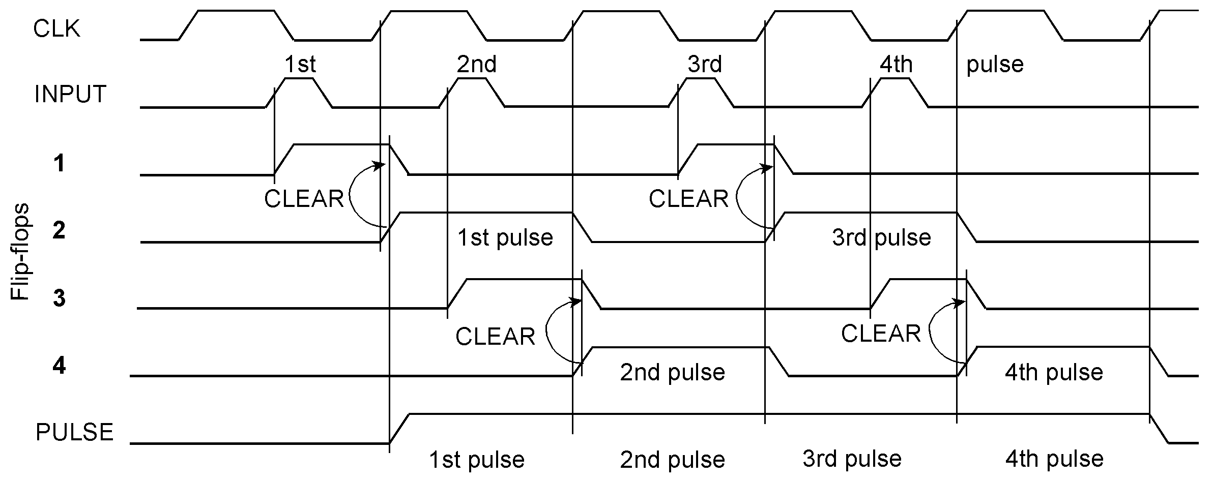
The circuit converts sequences of narrow pulses into an NRZ (Non-Return-to-Zero) representation. Two consecutive narrow pulses will cause an output pulse two clock cycles wide. More consecutive pulses will produce an appropriately wider output pulse. Here, four arriving pulses cause an output pulse four clock cycles long:
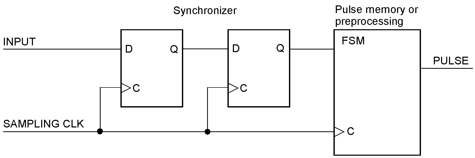
The circuits shown above could be implemented by tiny logic or in CPLDs. They are adequate for asynchronous pulses down to tens of nanoseconds and frequencies up to some MHz. When the design task is more demanding, I recommend sampling and synchronizing the pulses by an appropriate high-frequency clock and solving the particular application task of memorizing, deglichting, and the like by a downstream finite state machine (FSM). The arriving pulses are sampled and synchronized. Here, a two-stage synchronizer is shown. The application problem can be solved by state machine design as taught in the textbooks and supported by hardware description languages (HDLs) and integrated development systems.
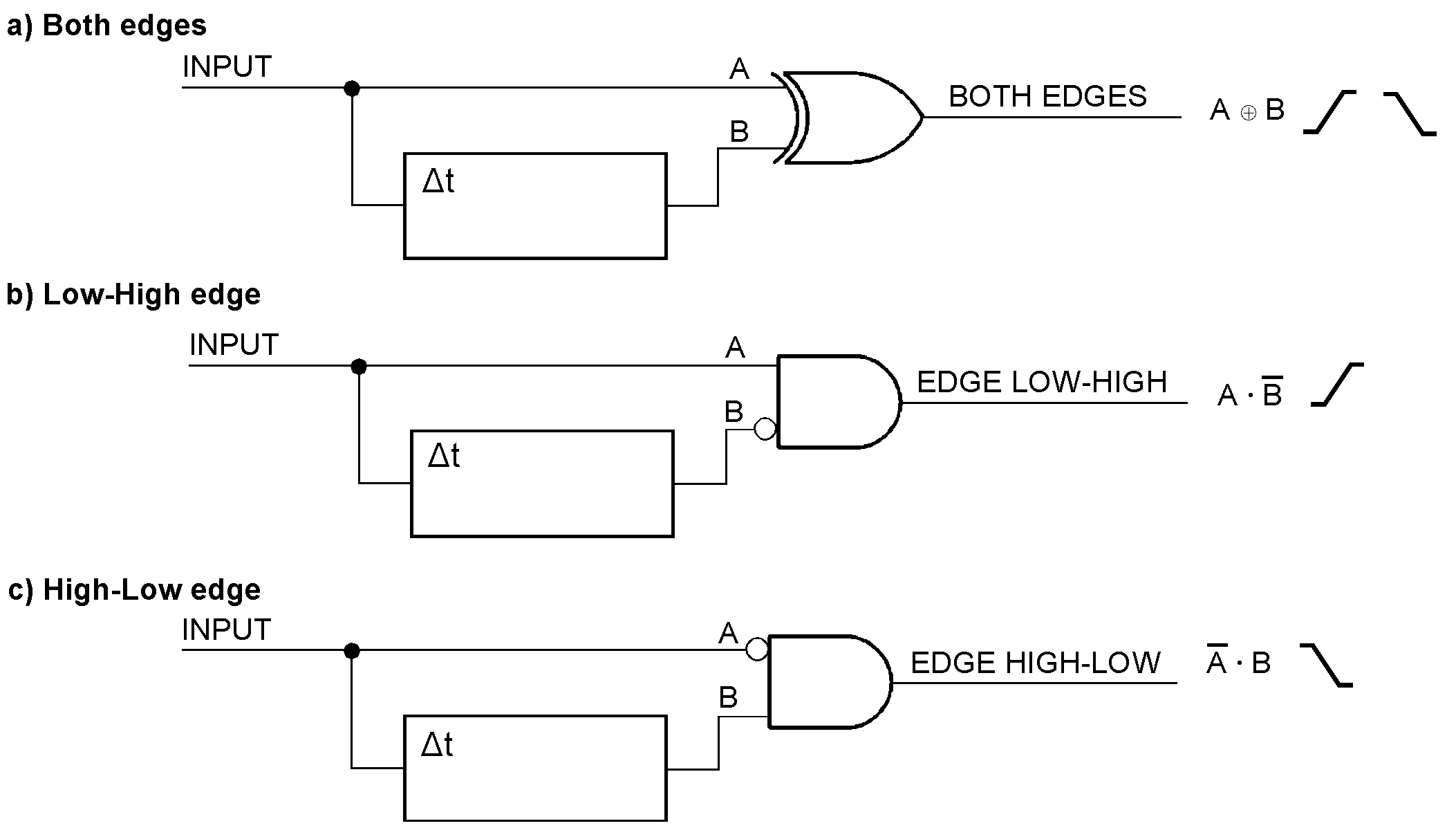
Detecting complete pulses The circuit (a) detects both edges regardless of how they follow each other. The circuits (b) and (c) detect pulses beginning with a Low-to-High or High-to-Low edge, respectively.
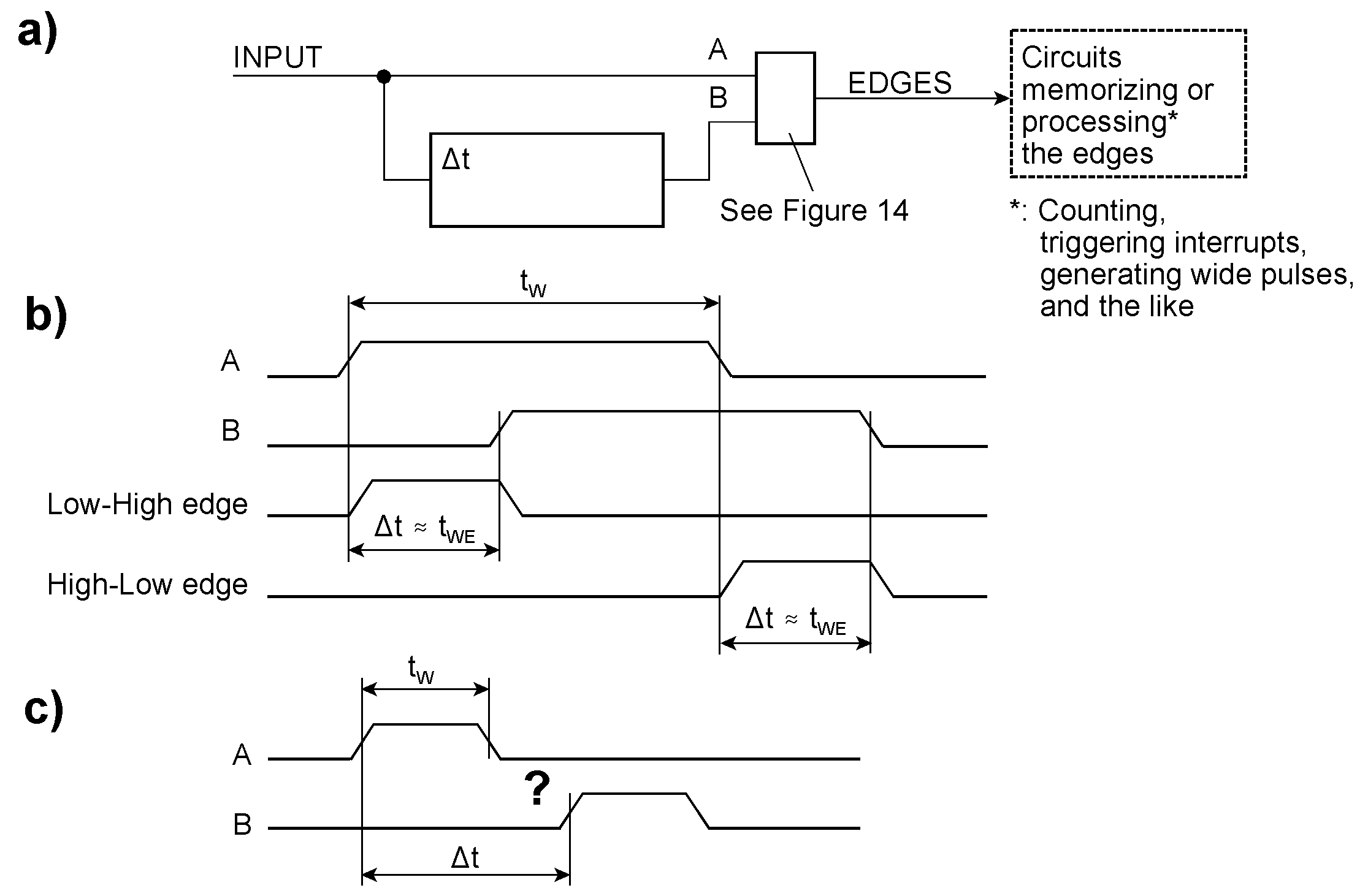
Detecting edges An alternative approach is to delay the signal and compare the delayed level with the current one). The limiting parameters are the minimum pulse width tW in the pulse train and the minimum pulse width tWE that the edge detector circuits expect. tWE approximately equals the delay time Δt. The delay must be shorter than the pulse ( Δt < tW); otherwise, the circuit will not work. Edge detection by delaying. (a) depicts the principal circuit, (b) how both edges are detected. (c) illustrates that the circuit will not work when the arriving and the delayed pulse do not overlap.
Basic edge-detection circuits:.
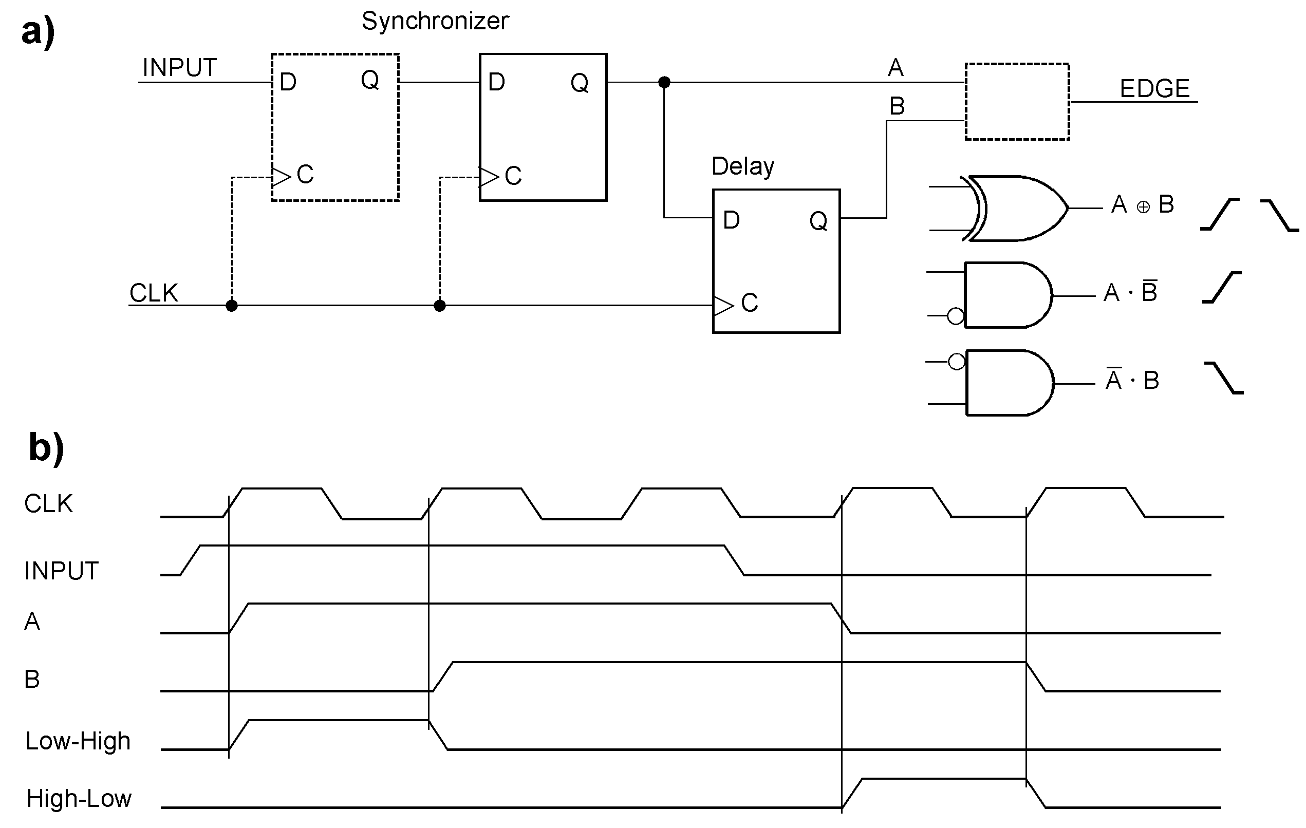
The output signals are typically pulses slightly shorter than the delay time Δt. Because Δt must be beyond the minimum width of the input pulses, the output pulses will be conspicuously narrow. In many application circuits, they must be stretched or memorized. There are various principles to delay a signal. It can be done by analog or digital components. When the arriving pulses are particularly narrow (think of micro- or even nanoseconds), it might be appropriate to implement the edge detection in the asynchronous domain, perhaps by analog circuits, and provide a fast pulse-capturing or single-shot circuit downstream. In a synchronous clock domain, the most straightforward digital delay component is the D-type flip-flop. A D-type flip-flop delays the synchronous pulses. The edges are signaled by output pulses being a single clock cycle wide. If wider output pulses are needed, several delaying flip-flops could be connected in series (that is, as a shift register), provided the pulses of the input pulse train are wide enough (that is, wider than the delay).
Pulse stretching and recovery
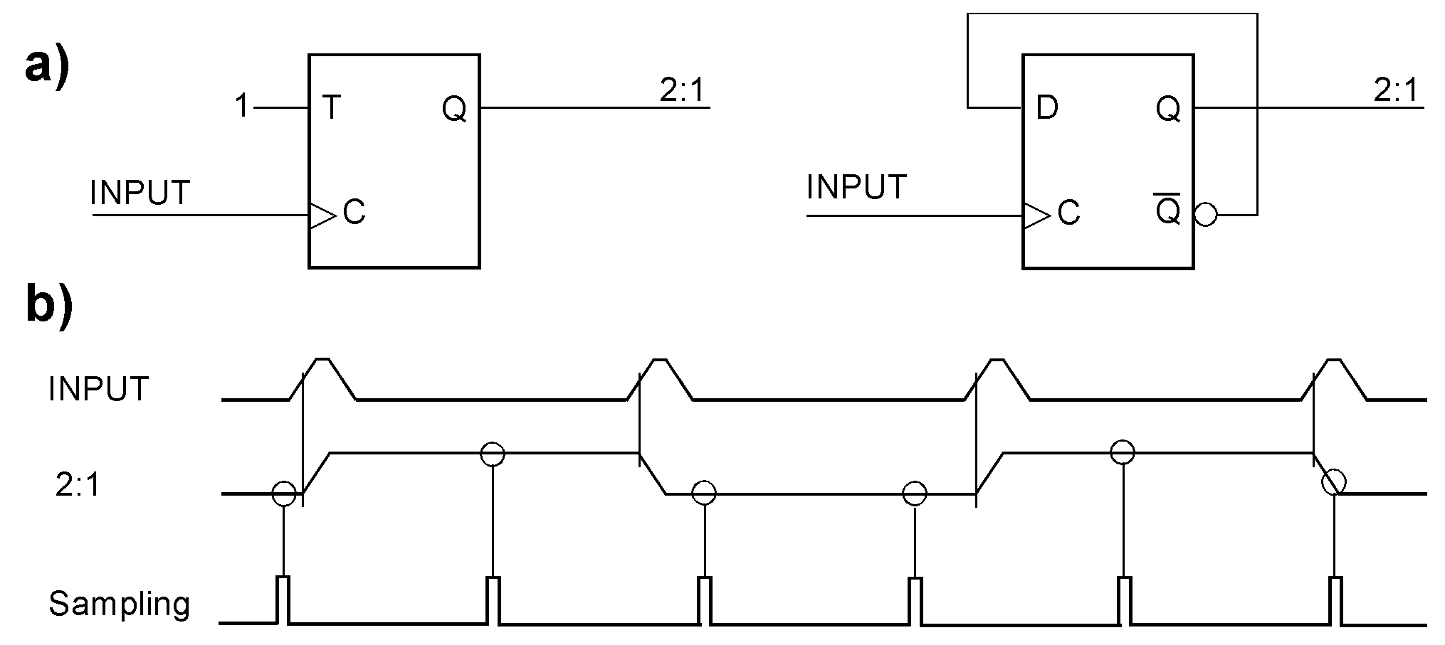
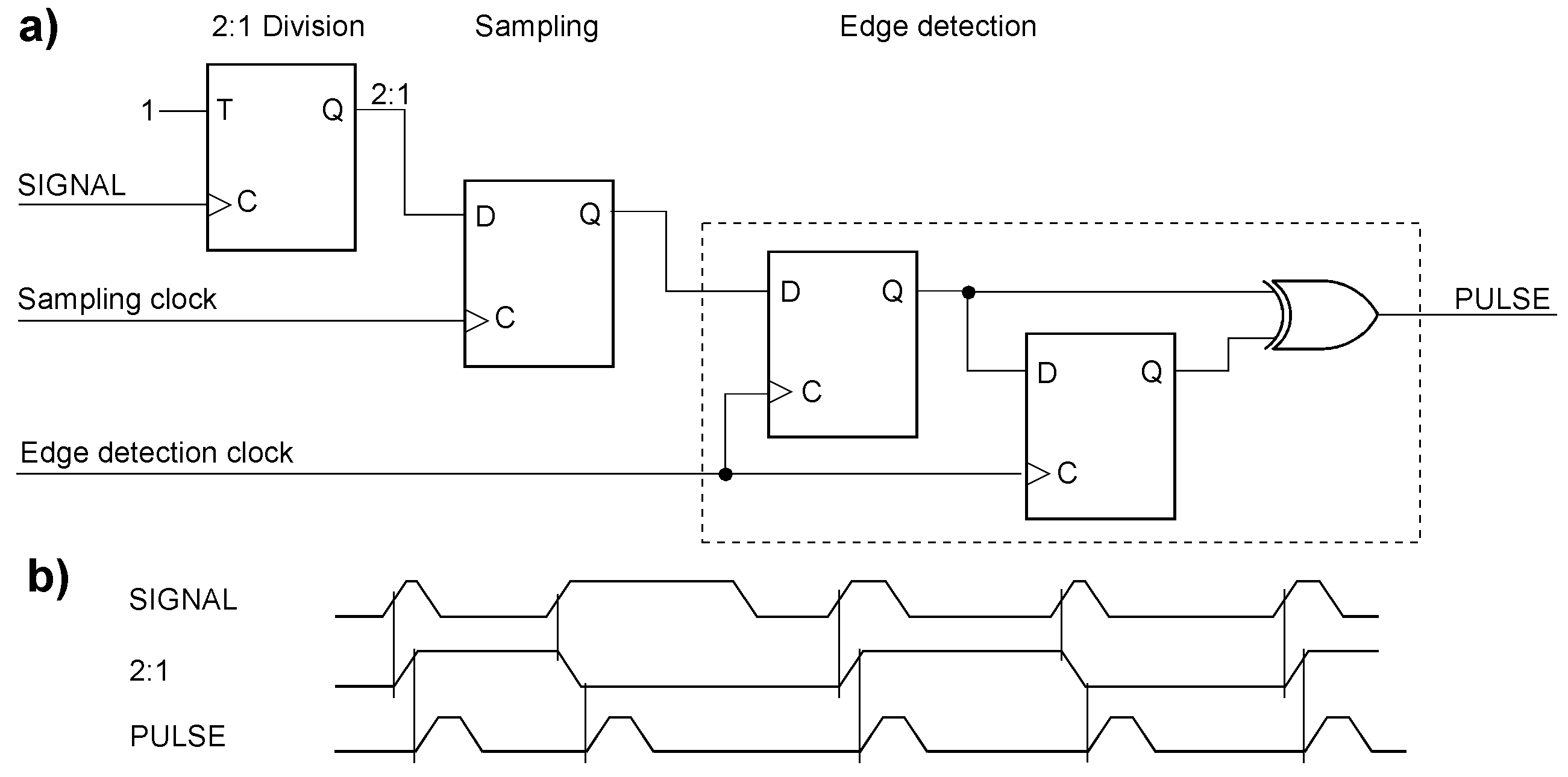
Each edge of the 2:1 pulse train signals an original pulse. Hence, the original pulse train can be reconstructed by detecting both edges. Here, it is done by a synchronous edge detector (a). Its clock determines the width of the output pulses. The delay must be shorter than the narrowest pulse. Therefore, the edge detection clock frequency must be higher than the sampling clock frequency. To ensure this, the sampling clock could be, for example, derived from the edge detector’s clock by frequency division. (b) shows example waveforms. A practical application example is crossing clock domains. The SIGNAL comes from another clock domain. This pulse train is injected into the target clock domain, to which the sampling and edge detection clocks belong.
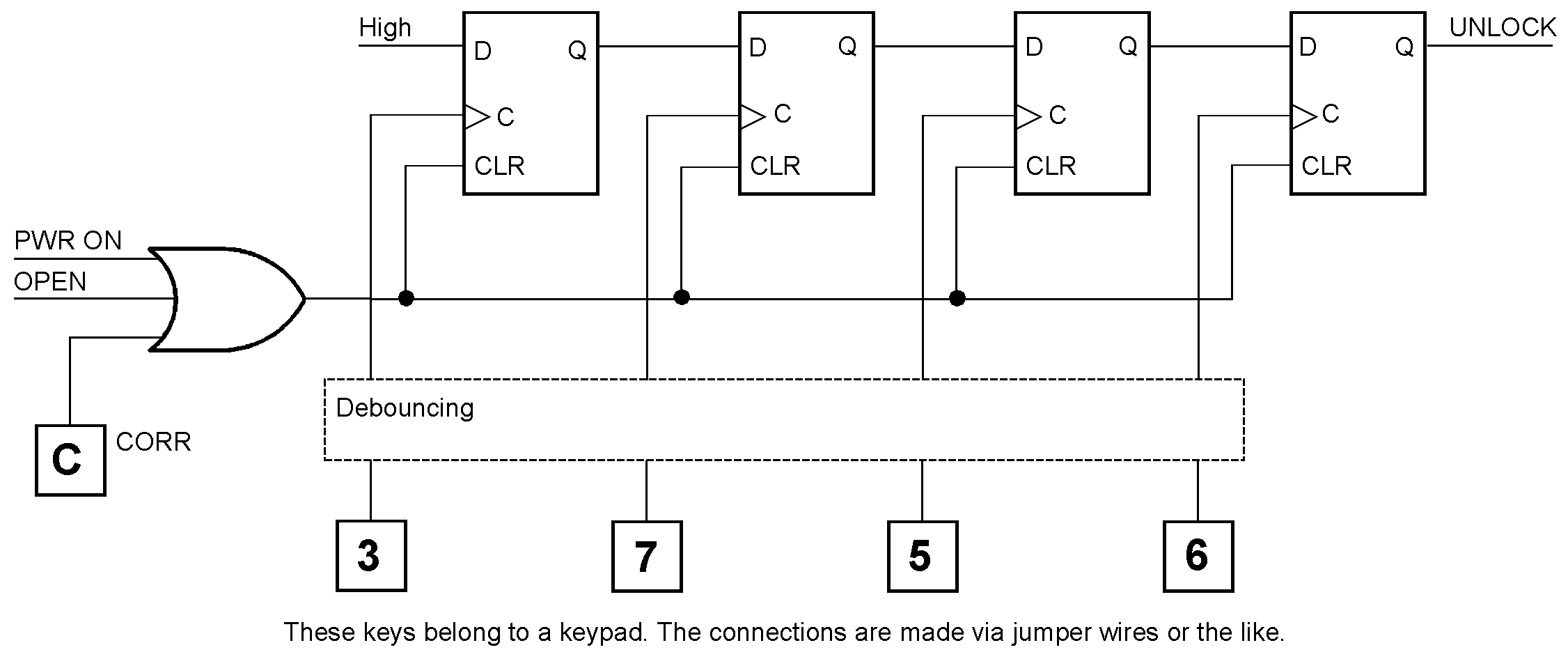
Detecting sequences Sequence detection shown by the example of a straightforward code lock. The UNLOCK signal actuates the door opener. The flip-flops are cleared during power-on, when the door has been opened, or when the CORR key is depressed. The number keys are part of a keypad (with the keys 0...9; arrangement similar to a telephone or calculator). The key signals must be bounce-free. For the UNLOCK output signal to become active, the number keys 3, 7, 5, and 6 must be pressed in precisely this order. If the door has been opened, the OPEN signal activated by a door contact resets the code lock.
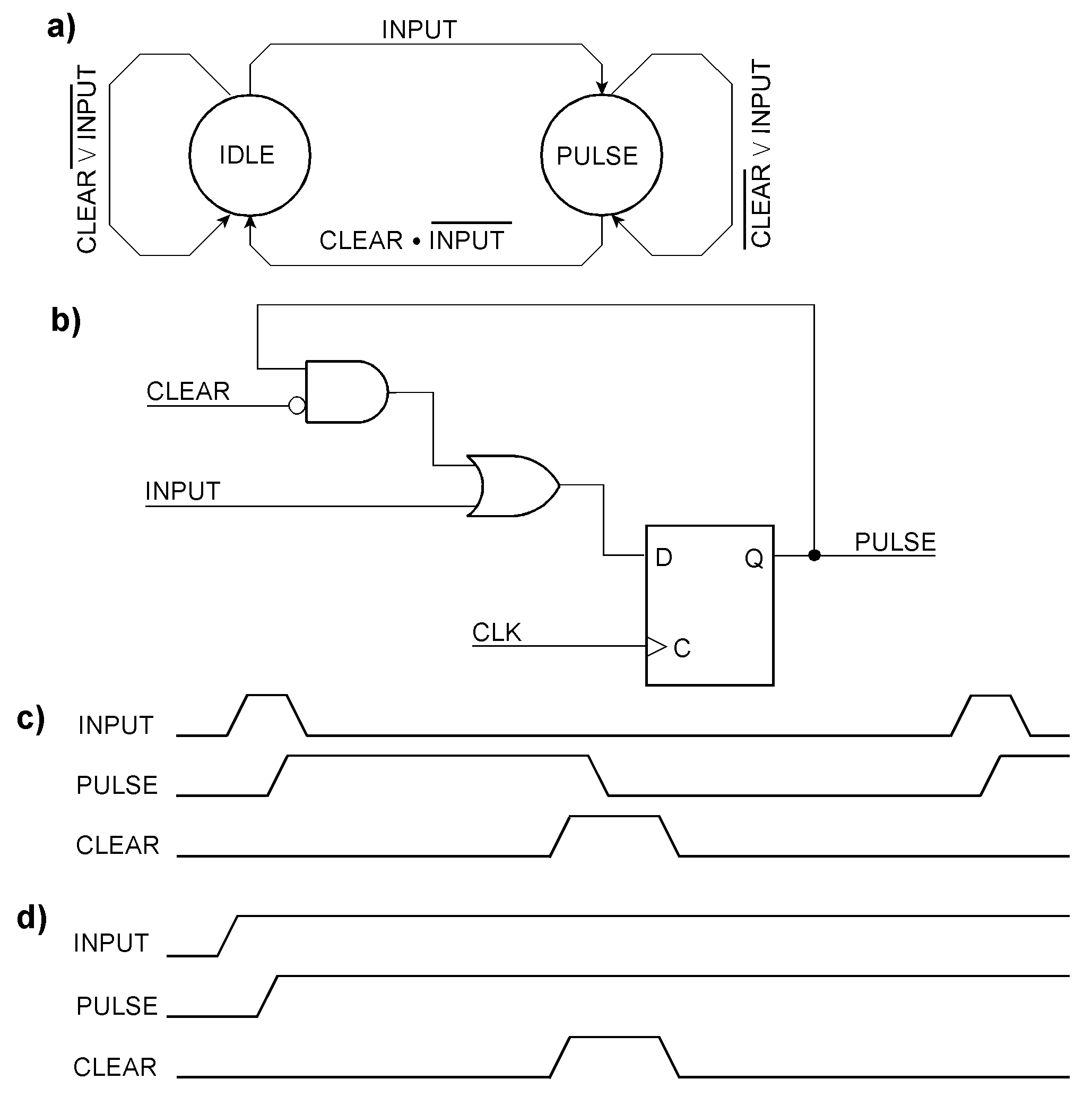
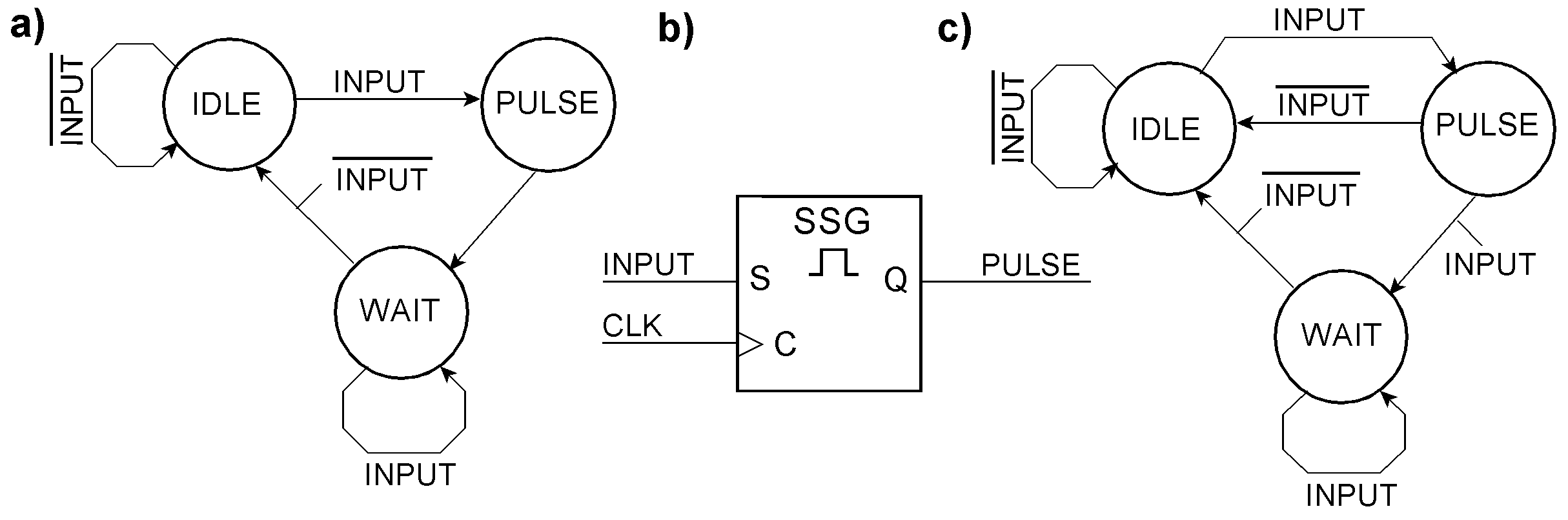
By the way, the circuit is simple but dangerous. As brain teasers: (1) How can you crack such a lock? (2) How can you detect and prevent cracking? Capturing pulses synchronously Basic capturing tasks Synchronous pulse memories The most straightforward FSMs have only two states. When the arriving pulses and clearing of the pulse memory do not overlap, we can get by with an IDLE state, when nothing is to memorize, and a PULSE state, if the input has become active. When the input pulse has disappeared, the feedback will cause the PULSE state to be retained until CLEAR becomes active and disconnects the feedback. Thus, the pulse memory will fall back to its IDLE state. If, however, CLEAR is asserted while INPUT is active, the latter will take precedence, causing the FSM to remain in the PULSE state. This synchronous pulse memory detects the signal level. The pulse input takes precedence over CLEAR. a) state diagram; b) circuit example. c) A short pulse is memorized and then cleared. d) If the pulse input is permanently active, CLEAR does not affect the PULSE state. An illustrative application example is the capturing of an error signal. If PULSE diminishes after asserting CLEAR, it is a transient error; if not, it is a permanent fault.
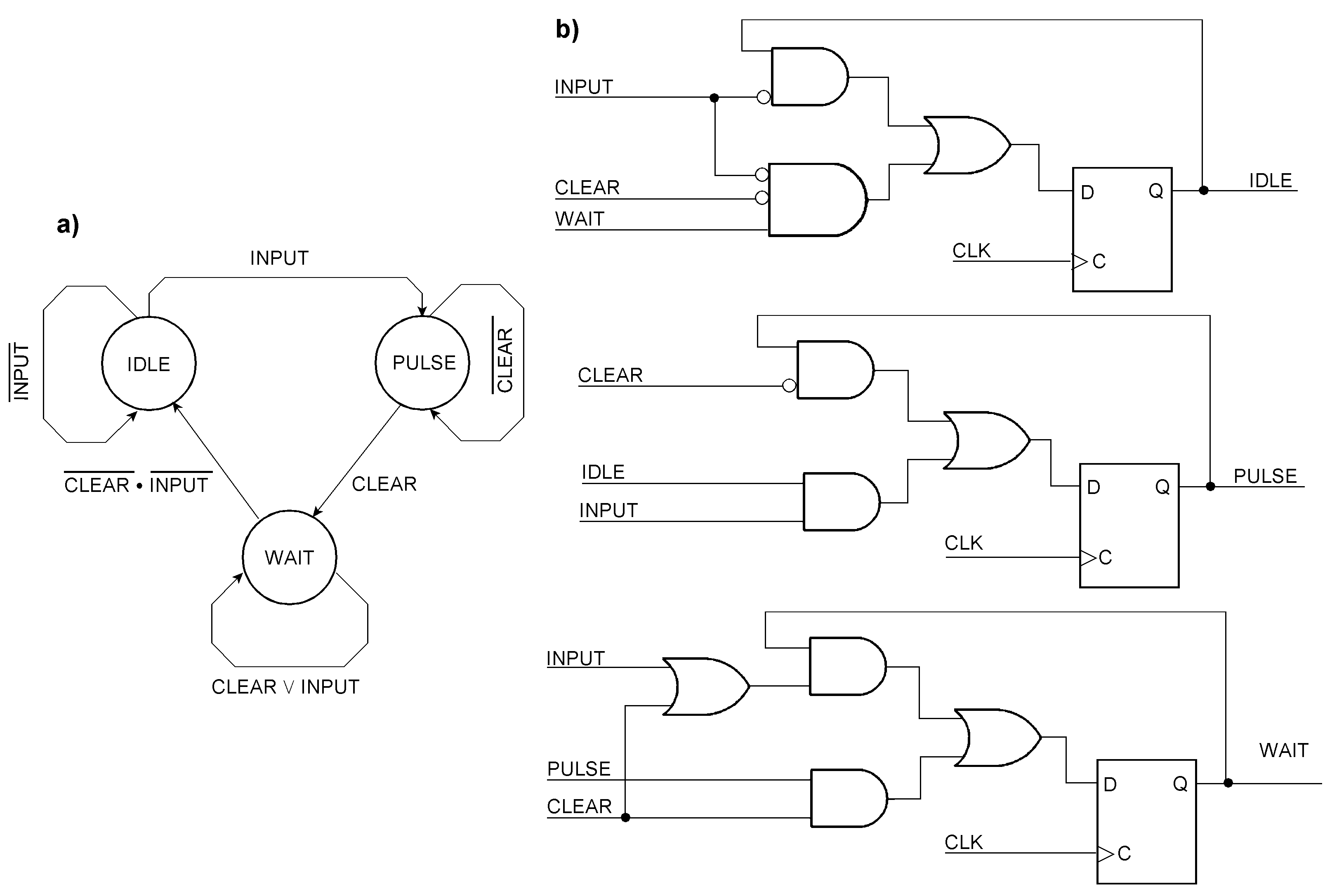
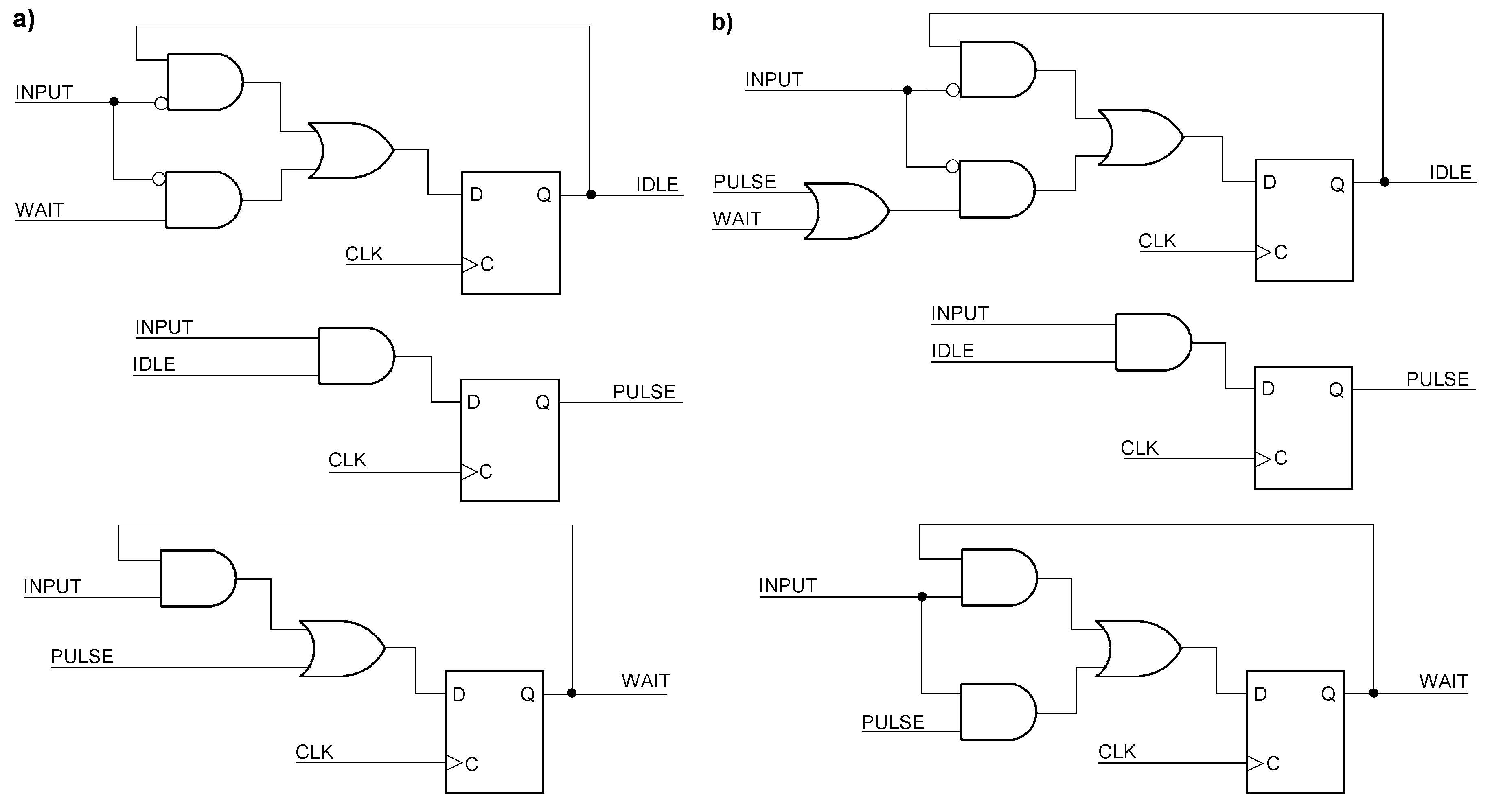
This synchronous pulse memory detects the pulse’s Low-to-High edge. It will accept a pulse only when both signals, INPUT and CLEAR, have been inactive together previously. For this, a third state has been added to wait for the said condition. The IDLE state will only be taken again after the input pulse and the CLEAR signal have both become inactive. Afterwards, the FSM is armed again to catch the next arriving pulse. CLEAR takes precedence over the pulse input. After the CLEAR signal has been deasserted, the circuit will wait until the pulse input becomes inactive (Low) too. a) state diagram; b) circuit example. The state encoding is one-hot enable (OHE). On power-on, IDLE must be set; PULSE and WAIT cleared.
Example single-shot generators Principles of synchronous single-shot pulse generation. a) state diagram; b) circuit symbol; c) modification for skipping the WAIT state if the input signal becomes inactive while still in the PULSE state. Each state transition requires one clock cycle. When the input signal is asynchronous, it must first be synchronized. When it could be affected by glitches or bouncing, it must be debounced, to boot. According to state diagram (a), the FSM will always go through the wait state, even if the input signal has already become inactive. The stae diagram (c) shows how, in this case, the wait state can be skipped.
Single-shot pulse generation by OHE-encoded FSMs. On power-on, IDLE must be set; PULSE and WAIT cleared. a) implements the state diagram (a) b) the stae diagram (c)shown above.
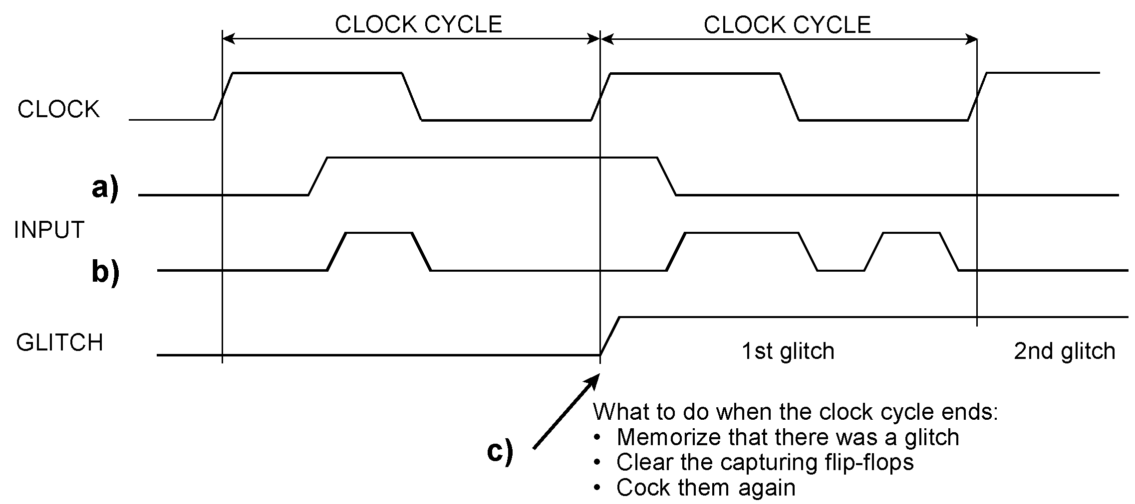
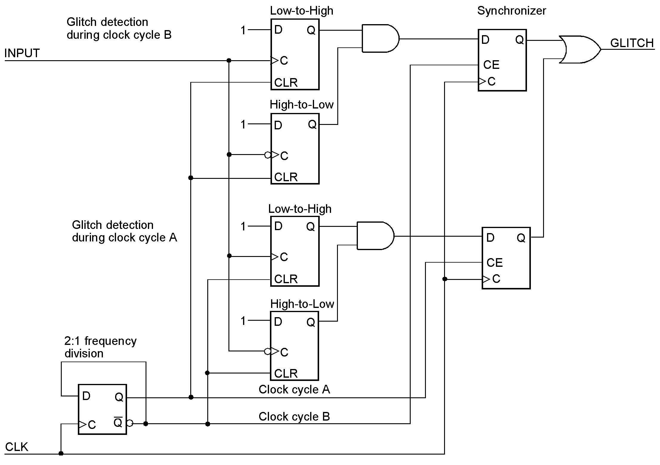
Glitches There are two principal definitions of what constitutes a glitch. According to the "asynchronous" definition, a glitch is any pulse narrower than a specified (short) time. The "synchronous" definition relates to a specified clock cycle. A glitch is a complete pulse (more generally, any waveform showing at least two edges) during a clock cycle. Oscilloscopes see asynchronous, logic analyzers see synchronous glitches. Detecting asynchronous glitches in a synchronous enviroment Detecting asynchronous glitches occurring within clock cycles. The input pulse (a) shows only one edge in each clock cycle. Hence, it is not a glitch. In contrast, the pulse train (b) carries glitches during two adjacent clock cycles. The arrow (c) points to the end of a clock cycle and the beginning of the next. In this moment, the stipulated activities of meorizing, clearing, and cocking again are to be carried out. Detecting edges is easy. It could be done by edge-triggered flip-flops. However, the clock cycles follow one another without any gaps. (c) shows what to do at the moment of the transition from one clock cycle to the next. Because we use the clock inputs of our capturing flip-flops to detect glitches, synchronous operation is out of the question. What we cannot do is resort to advanced transistor-level design, like the manufacturers of digital storage oscilloscopes and logic analyzers. Instead, we can only think of straightforward circuits built by readily available components. Seamless glitch detection in a synchronous environment. Two circuits in teeter-totter operation ensure that no glitch escapes capturing. Two detection circuits, each consisting of two pulse memories, are used alternately in successive clock cycles A and B. During clock cycle A, the lower detection circuit is active, and the upper one is held in reset. During clock cycle B, the modes of operation are reversed. When changing from one clock cycle to another, the output signal of the respective detection circuit is transferred to a synchronization flip-flop.
A legacy debouncing synchronizer
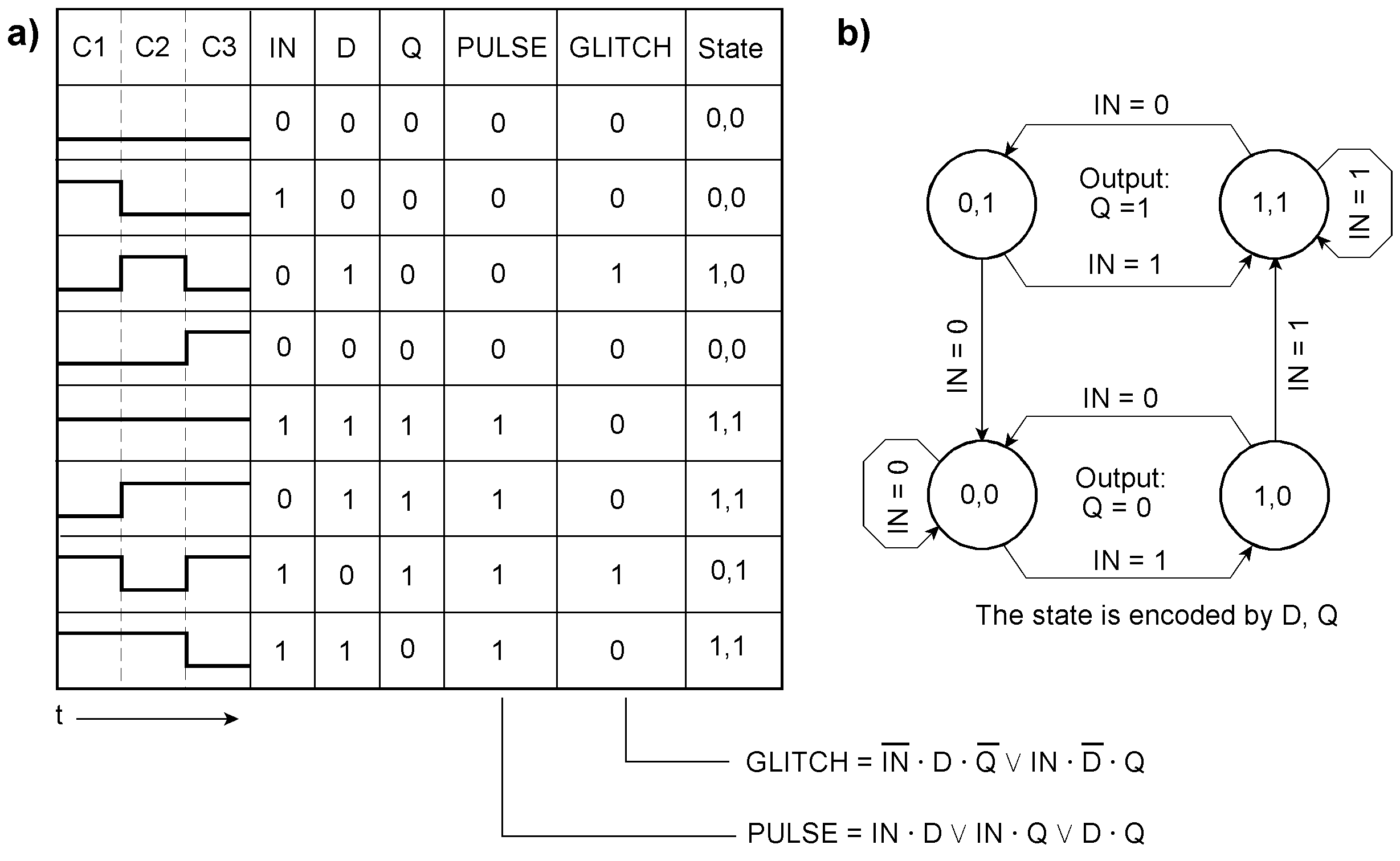
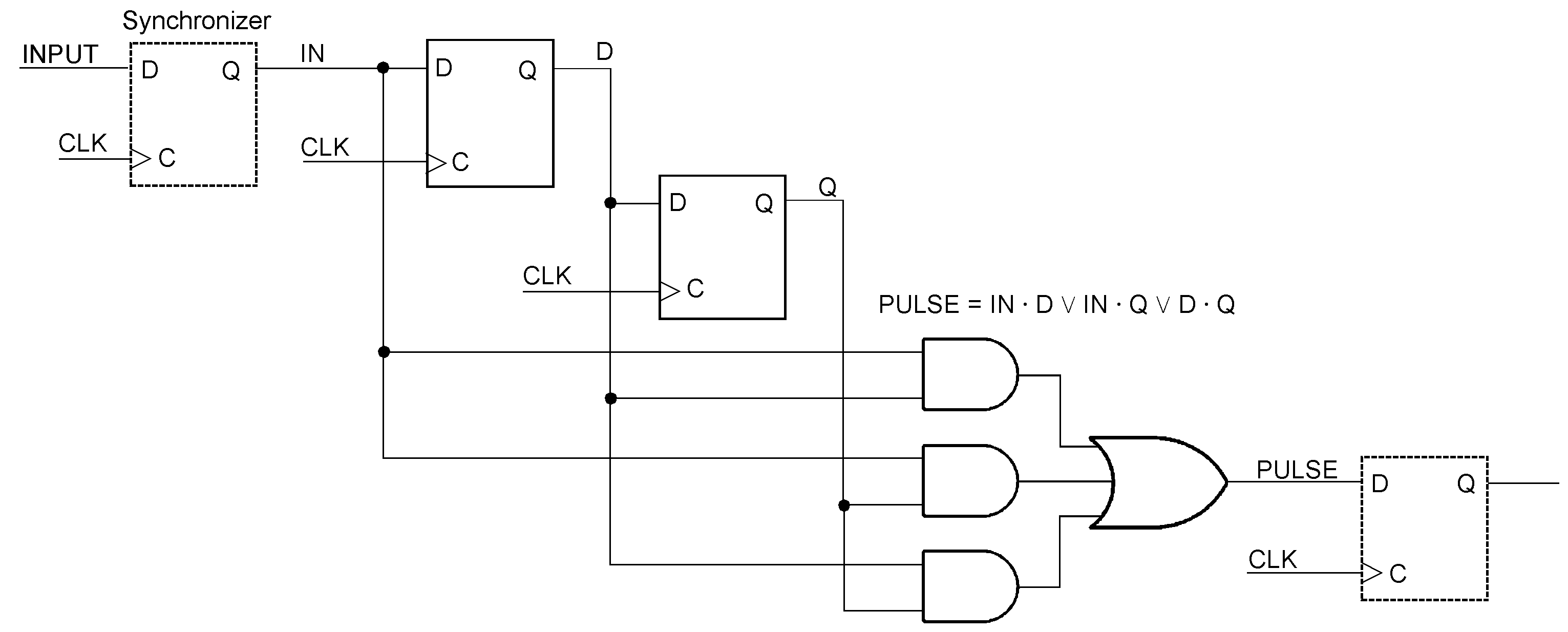
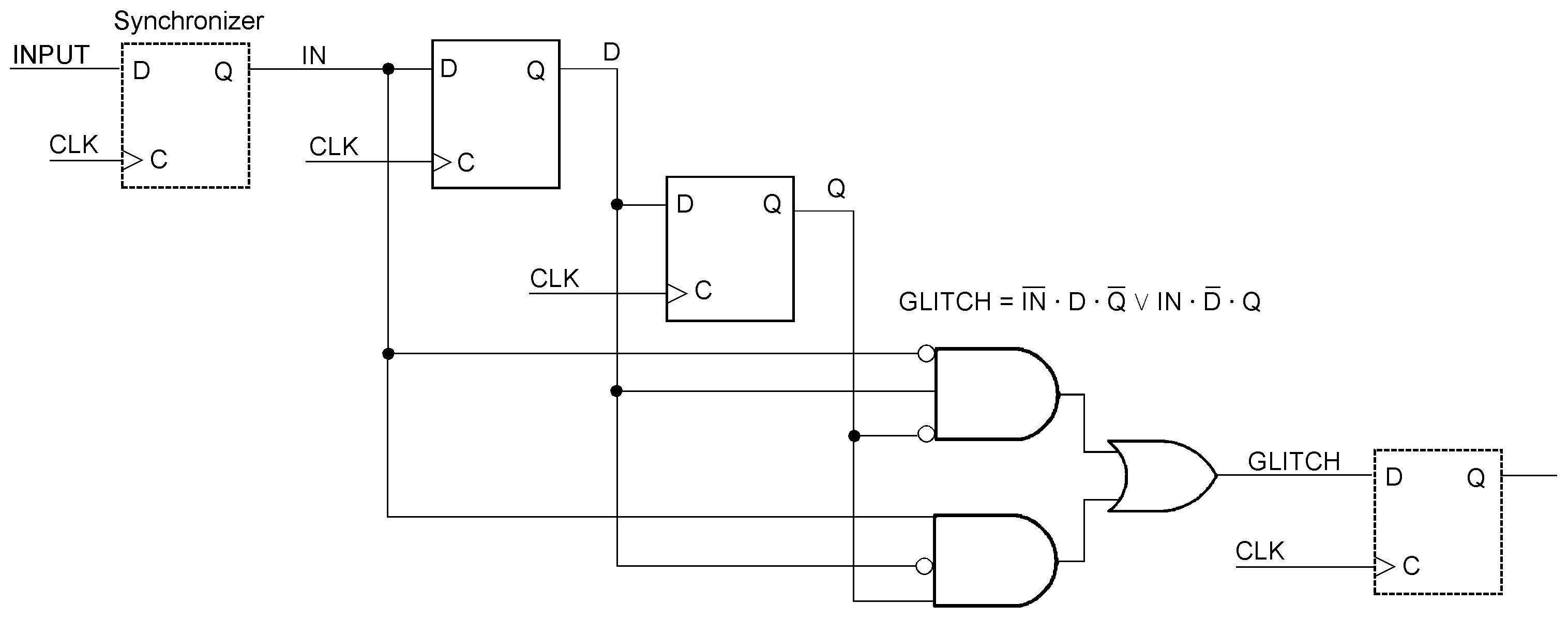
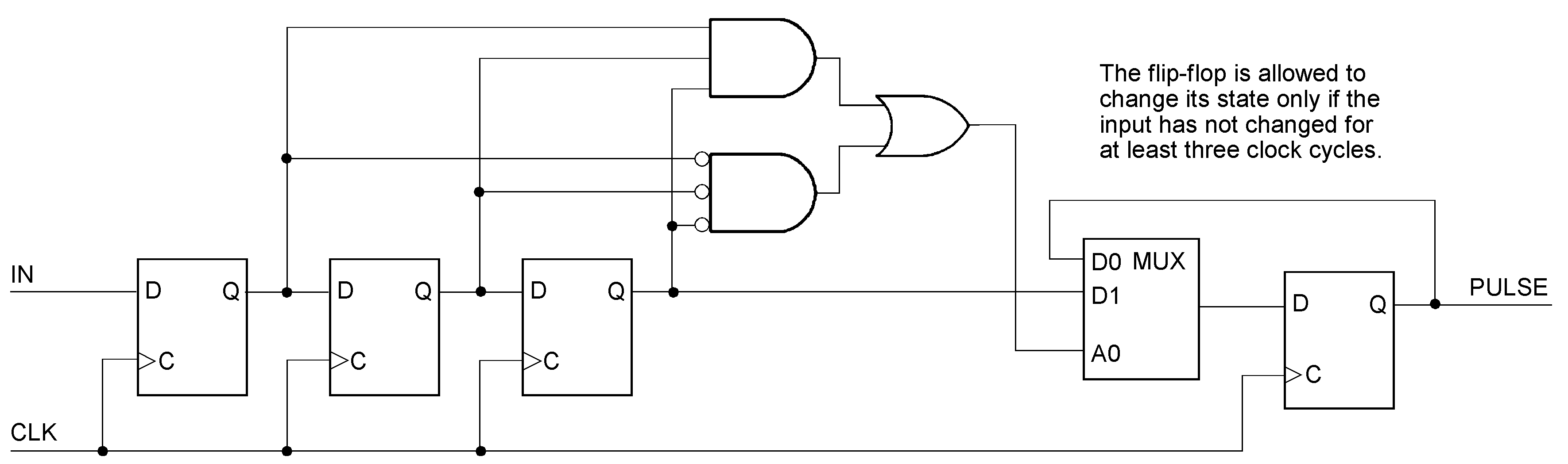
The too-narrow pulse (1) does not coincide with a low-to-high edge of the clock. Hence, it will not be synchronized. The too-narrow pulse (2) is captured but will clear the pulse memory flip-flop during the current clock cycle. Hence, it will not be synchronized. In contrast, the pulse (3) is wide enough. It is held in the pulse memory flip-flop until the next Low-to-High edge of the clock and thus synchronized. If the pulse is slightly wider than one clock cycle, it may be synchronized or not. To be synchronized, it must remain active until the next Low-to-High clock edge. If the pulse is somewhat wider than two clock cycles, it will be reliably synchronized. The circuit is only usable if it does not matter whether pulses wider than one but narrower than two clock periods are being synchronized or not. A typical application example is contact debouncing, where the clock can be generated even by software (we speak of cycles in the magnitude of some milliseconds here). The circuit we call venerable because of its age. Due to its age, however, there is also a caveat. Decades-long experience has shown that it works well, for example, with the SN7474 D-type flip-flop. However, when implemented by up-to-date components, it may not work faultlessly. It could even be possible that the integrated development environment (IDE) refuses to synthesize it. The cause is that the INPUT signal acts upon the synchronous D as well as the asynchronous CLR input of the pulse memory flip-flop. Synchronous deglitching and glitch detection If the pulse is narrower than a clock cycle, it is considered a spike or glitch; if wider, it is considered acceptable. Therefore, choose the clock frequency according to the pulse width that makes the difference between a glitch and an acceptable pulse. In a completely synchronous circuit, the signals to be evaluated are already synchronized. We assume a synchronization clock cycle corresponding to the maximum width that is considered to be a glitch. Then, a glitch corresponds to a one between two zeros or a zero between two ones. Consequently, acceptable pulses consist of at least two consecutive zeros or ones. Successive snippets of a pulse train can be sequentially memorized using flip-flops connected in series. In the simplest case, three clock periods must be considered: the signal level synchronized in the current cycle and those of the two preceding cycles. To analyze the pulse patterns that might occur, we set up a truth table that contains all eight possible signal combinations (Figure 26). Synchronous glitch filtering and detection (based on [A4]). a) truth table, b) state diagram of the glitch filter’s finite state machine (FSM). The Boolean equations relate to the glitch filter and the glitch detector circuits shown below.
C1, C2, and C3 are the three successive clock cycles we want to observe. The truth table contains all eight possible pulse patterns. We begin at a Low level. Then a High glitch emerges, becomes visible, and diminishes again. The second half of the table begins at a High level. Then a Low glitch emerges, becomes visible, and diminishes again. The FSM’s state is encoded by the flip-flops D and Q. In each clock cycle, the output depends on the input and the state. The input (IN) comes from the synchronizer. Because it is already clock-synchronous, we need only two state flip-flops. To suppress glitches, the circuit in Figure 27 will emit a zero if two or more zeros or a one if two or more ones follow each other. It will not change its output if a single one is interspersed between two zeros or a single zero between two ones. Precisely these conditions define a glitch. They are detected by the circuit in Figure 28. A glitch filter or de-glitching circuit based on the truth table above. It outputs a pulse train free of glitches.
A glitch detector circuit based on the truth table above. It outputs pulses representing glitches. Thus, they could be memorized, highlighted, counted, and the like.
Another glitch filter or de-glitching circuit shows an obvious, easy-to-understand principle of operation. The glitch filter consists of a shift register, a combinational circuit detecting particular bit patterns, and an output flip-flop. The pulse train is fed into the shift register. The output flip-flop may change its state only if the shift register contains three ones or zeros, thus suppressing all other bit patterns mentioned in zhe truth table above. The shift register’s output is then memorized in the output flip-flop.It is also obvious that it could be used to suppress wider glitches by simply making the shift register longer and the AND gates wider.
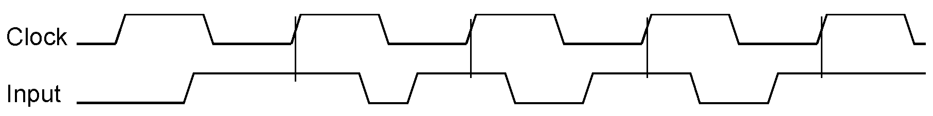
A crucial difference between asynchronous and synchronous glitch filtering These waveforms show the difference between asynchronous and synchronous de-glitching. Asynchronous and synchronous circuits will react differently.
If the input signal is fed to an asynchronous deglitching circuit, no pulse will appear on the output. If fed to the synchronous circuit shown avbove, however, a pulse will be output because three consecutive clock edges have sampled the same signal level. Therefore, analyze your application requirements carefully and be wise when selecting an appropriate circuit.
|
|
|
|
Download the Internet addendum to the CC article
|